P-type super-junction transverse double-diffusion metal oxide semiconductor tube

An oxide semiconductor, lateral double diffusion technology, applied in semiconductor devices, electrical components, circuits, etc., can solve problems such as depletion of P-type pillars and failure to fully deplete breakdown voltage at the same time

Inactive Publication Date: 2011-06-15
SOUTHEAST UNIV
View PDF3 Cites 6 Cited by
  • Summary
  • Abstract
  • Description
  • Claims
  • Application Information

AI Technical Summary

Problems solved by technology

However, there is a problem of substrate-assisted depletion of the P-type pillars in the traditional super-junction lateral double-diffused metal-oxide-semiconductor transistors, which leads to

Method used


Image

  • P-type super-junction transverse double-diffusion metal oxide semiconductor tube
  • P-type super-junction transverse double-diffusion metal oxide semiconductor tube
  • P-type super-junction transverse double-diffusion metal oxide semiconductor tube

Examples


Embodiment Construction

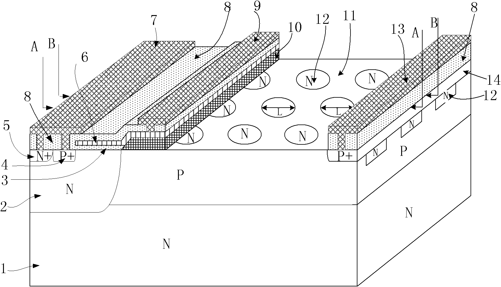
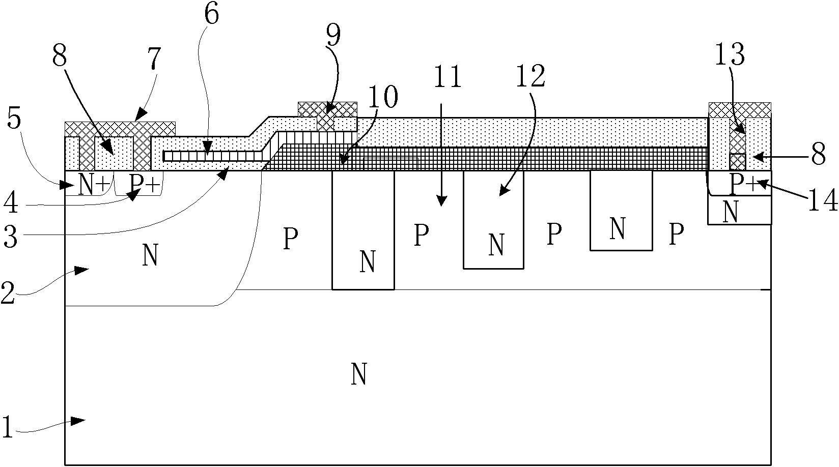
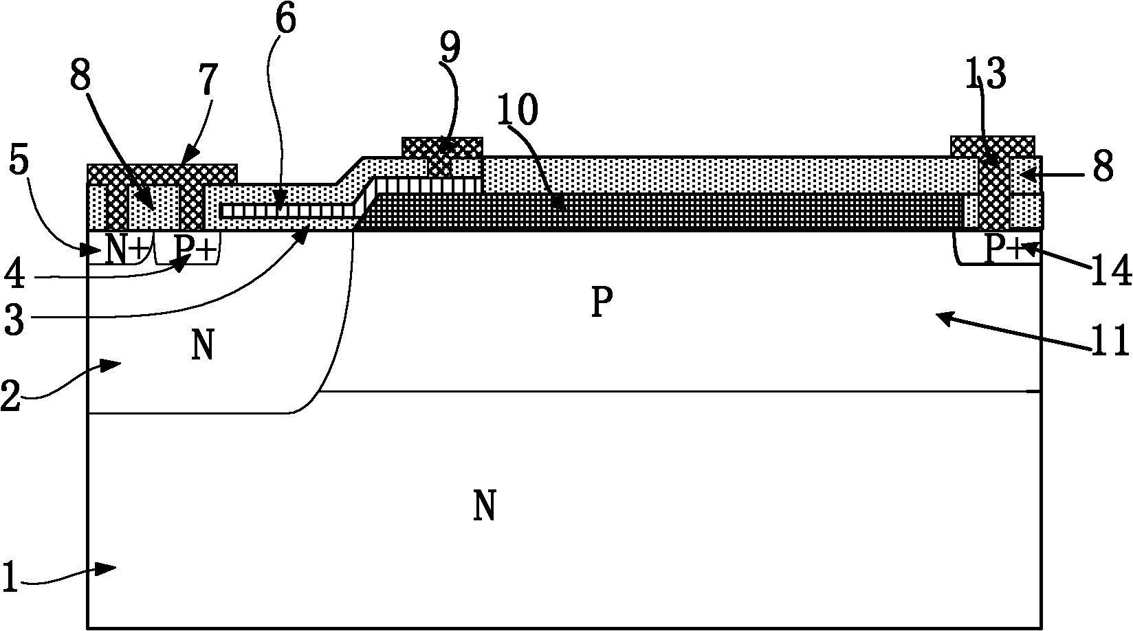
[0017] refer to figure 1 , a P-type superjunction lateral double-diffused metal oxide semiconductor transistor, comprising: an N-type substrate 1, a superjunction structure and an N-type body region 2 are arranged on the N-type substrate 1, and the superjunction structure is composed of a P-type epitaxial layer 11 and an N-type semiconductor region 12 embedded in the P-type epitaxial layer 11. A P-type source region 4, an N-type body contact region 5 and a gate oxide layer 3 are arranged above the N-type body region 2. In the super junction structure A P-type drain region 14 is arranged above the super junction structure, and a first-type field oxide layer 10 is arranged on the area outside the P-type drain region 14, and a polysilicon gate 6 and a polysilicon gate are arranged above the gate oxide layer 3. 6 extends from above the gate oxide layer 3 to above the first type field oxide layer 10, above the P type source region 4, the N type body contact region 5, the P type dr...


PUM


Abstract

The invention discloses a P-type super-junction transverse double-diffusion metal oxide semiconductor tube, which comprises an N-type substrate, wherein the N-type substrate is provided with a super-junction structure and an N-type body region; the super-junction structure consists of a P-type epitaxial layer and an N-type semiconductor region embedded therein; the N-type body region is provided with a P-type source region, an N-type body contact region and a grid oxide layer; the super-junction structure is provided with a P-type drain region; a first type field oxide layer is arranged above the super-junction structure and positioned in a region beyond the P-type drain region; a polycrystalline silicon grid is arranged above the grid oxide layer and extends to the upper part of the first type field oxide layer from the upper part of the grid oxide layer; a second type field oxide layer is arranged above the P-type source region, the N-type body contact region, the P-type drain region, the polycrystalline silicon grid and the first type field oxide layer; the P-type source region, the P-type drain region, the N-type body contact region and the polycrystalline silicon grid are all connected with a source metal lead, a grid metal lead and a drain metal lead; and the depth of the N-type semiconductor region in the super-junction structure is linearly reduced in the direction from the P-type source region to the P-type drain region.

Description

technical field [0001] The invention relates to a high-voltage power metal oxide semiconductor device made of silicon, more precisely, a high-voltage P-type superjunction lateral double-diffused metal oxide semiconductor transistor made of silicon. Background technique [0002] At present, power devices are more and more widely used in daily life, production and other fields, especially power metal oxide semiconductor field effect transistors, because they have faster switching speed, smaller drive current, and wider safe operating area , so it has been favored by many researchers. The power devices integrated in power integrated circuits mainly include lateral insulated gate bipolar transistors and lateral double-diffused semiconductor metal oxide transistors. Although the current driving capability of lateral insulated gate bipolar transistors is relatively strong, the speed of power integrated circuits using lateral insulated gate bipolar transistors is limited due to th...

Claims


Application Information

Patent Timeline
IPC IPC(8): H01L29/78H01L29/06
Inventor 时龙兴华国环朱奎英李明钱钦松孙伟锋陆生礼
Owner SOUTHEAST UNIV
Why Eureka
Try Eureka