Manufacturing process of waveguide slot

A production process and waveguide groove technology, applied in the field of PCB board manufacturing, can solve the problems of complex manufacturing process, poor control of film pattern transfer and ink exposure and curing, and inability to guarantee quality, so as to achieve simple production process, low cost, and guaranteed quality. Effect

Active Publication Date: 2011-06-29
SHENNAN CIRCUITS
View PDF5 Cites 23 Cited by
  • Summary
  • Abstract
  • Description
  • Claims
  • Application Information

AI Technical Summary

Problems solved by technology

[0014] From the above description, it can be known that the waveguide groove manufacturing process uses LPI liquid photosensitive ink, but the manufacturing process is complicated, involving ink printing, exposure, development, curing and ink removal at the bottom of the groove. Since the ink is printed in the groove, plus Due to the limited exposure characteristics of the exposure lamp, the transfer of film graphics and the exposure and curing of ink are very difficult to control, so the quality cannot be guaranteed

Method used


Image

  • Manufacturing process of waveguide slot
  • Manufacturing process of waveguide slot
  • Manufacturing process of waveguide slot

Examples


Embodiment Construction

[0037] In order to make the object, technical solution and advantages of the present invention clearer, the present invention will be further described in detail below in conjunction with the accompanying drawings and embodiments. It should be understood that the specific embodiments described here are only used to explain the present invention, not to limit the present invention.

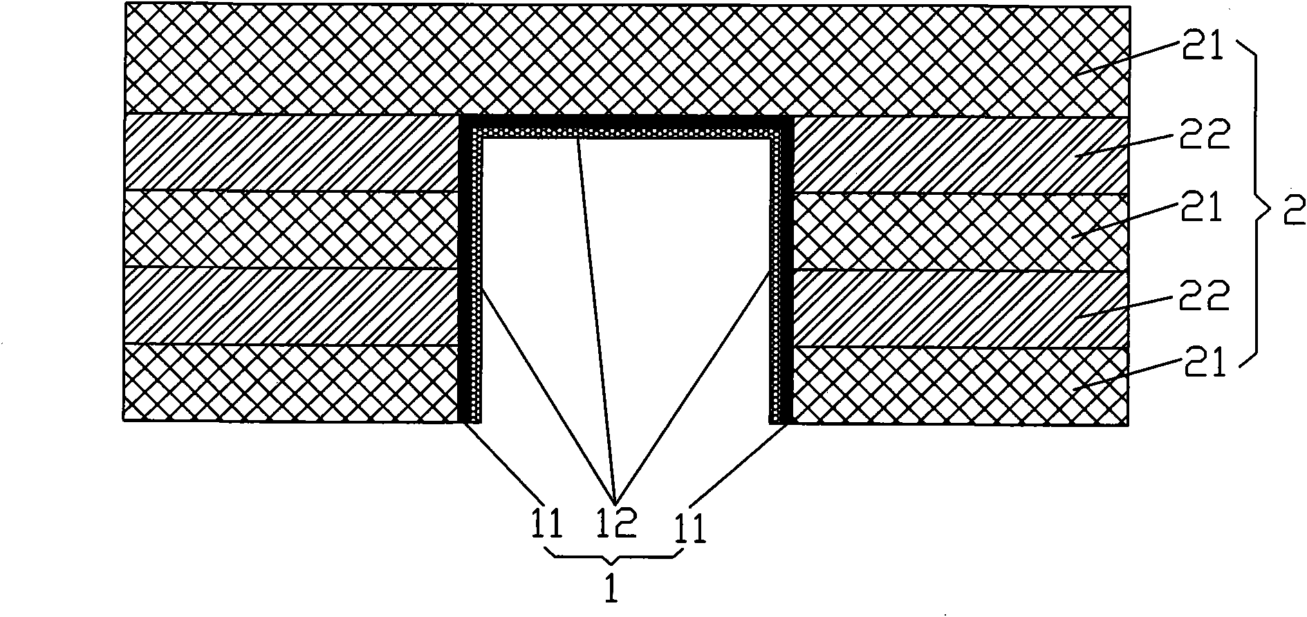
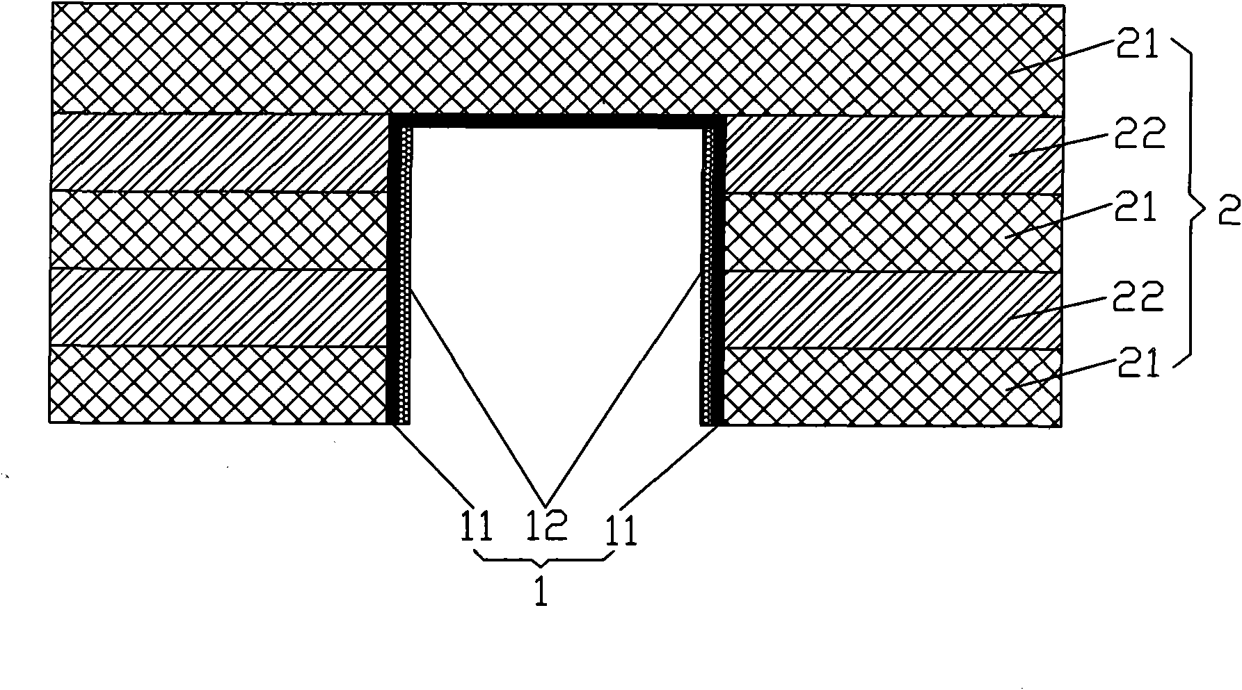
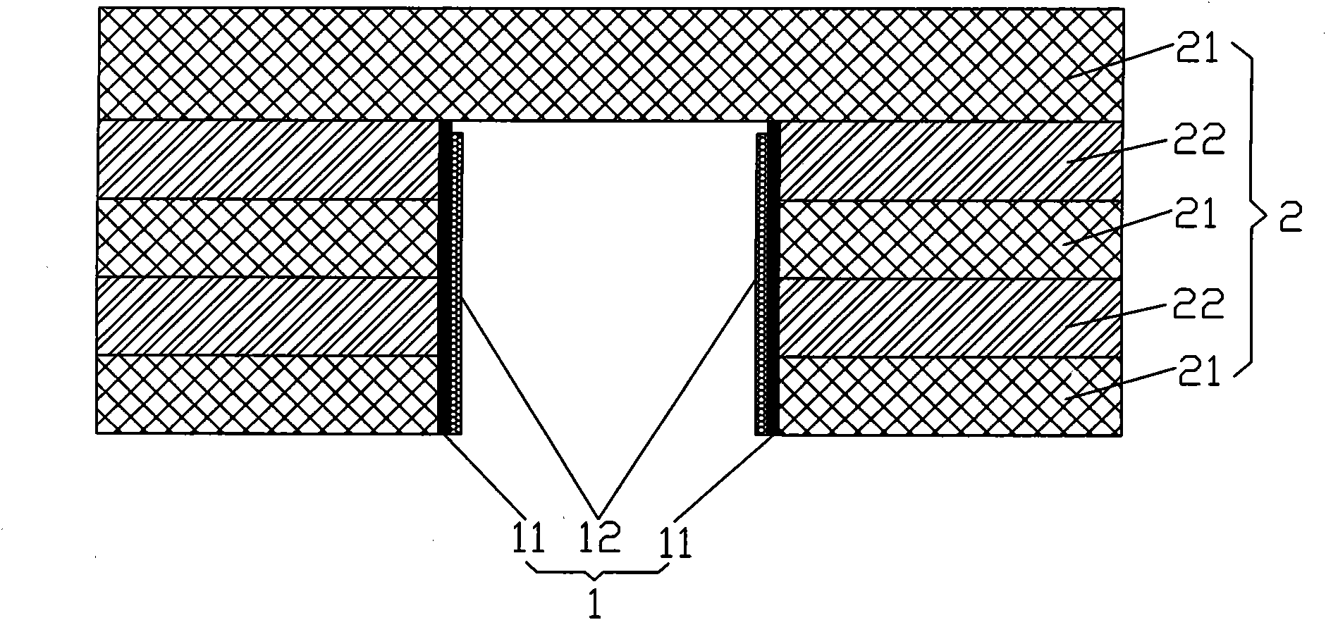
[0038] like Figure 1~4 As shown, a kind of waveguide groove manufacturing process that the embodiment of the present invention provides, described waveguide groove is the groove 1 that offers on PCB board 2, and the side wall of described groove 1 is copper-plated layer 11 and protective layer (Fig. Not shown in ), there is no metal layer at the bottom, and the PCB board 2 is made by stacking the core board 21 and the prepreg 22 in sequence, and its manufacturing process includes the following steps:

[0039] (1) Process the groove 1 on the PCB board 2. The processing technology of the groove 1 i...


PUM


Abstract

The invention provides a manufacturing process of a waveguide slot, which is suitable for the manufacturing field of a PCB board. In the manufacturing process provided by the invention, a tin coating which is disposed outside the bottom of a groove is burn off by laser while a copper coating inside the bottom of the groove is not removed due to the difference between the absorption rates of tine and copper to laser and the difference between the energy requirements for burning tin and copper with laser, so that the laser can be prevented from reaching to a core plate under the copper coating;then the copper coating inside the bottom of the groove is removed by etching, a tin coating disposed outside the side wall of the groove is removed by means of a common process method, a protection player is subsequently coated on a copper coating which is disposed inside the side wall of the groove, so that a waveguide slot of which the side walls are provided with metal layers (a copper coating and a protection layer) and the bottom does not have a metal layer. According to the invention, the manufacturing is simple, a liquid photoimageable (PLI) type printing ink step of the existing technology is replaced by a laser drilling step, the cost is relatively low, the position accuracy of the laser drilling machine is high, the quality of the waveguide slot can be ensured completely, so the volume production of the product can be carried out.

Description

technical field [0001] The invention belongs to the field of PCB board manufacturing, and in particular relates to a waveguide groove manufacturing process with metallized side walls and non-metallized bottoms. Background technique [0002] In the PCB board manufacturing industry, the waveguide groove is a groove opened on the PCB board. The side wall of the waveguide groove is a copper plating layer and a protective layer (collectively referred to as a metal layer). There is no metal layer at the bottom, and the metal layer on the side wall of the waveguide groove is used. It is used to shield the signals sent by the components on the PCB to prevent signal loss, while the bottom does not shield the signals to ensure the normal transmission of the signals. The structure of the waveguide groove can make the signal resonate. Therefore, this waveguide groove is in the industry. will be widely used. [0003] In the prior art, the manufacturing process of the waveguide groove is...

Claims


Application Information

Patent Timeline
Patent Type & Authority Applications(China)
IPC IPC(8): H01P11/00
Inventor 袁为群孔令文彭勤卫
Owner SHENNAN CIRCUITS
Why Eureka
Try Eureka