

Method for enhancing reliability of SONOS (Silicon Oxide Nitride Oxide Semiconductor) flash memory device by means of selective epitaxy
A flash memory device, a selective technology, applied in the direction of electrical solid-state devices, semiconductor devices, semiconductor/solid-state device manufacturing, etc., can solve the problems of increasing device performance instability, reducing device reliability life, silicon surface damage, etc., to achieve reliable Increased performance life, improved reliability, and ease of integration
- Summary
- Abstract
- Description
- Claims
- Application Information
AI Technical Summary
Problems solved by technology
Method used
Image

Examples
Embodiment Construction
[0015] The present invention will be described in further detail below in conjunction with the accompanying drawings and embodiments.
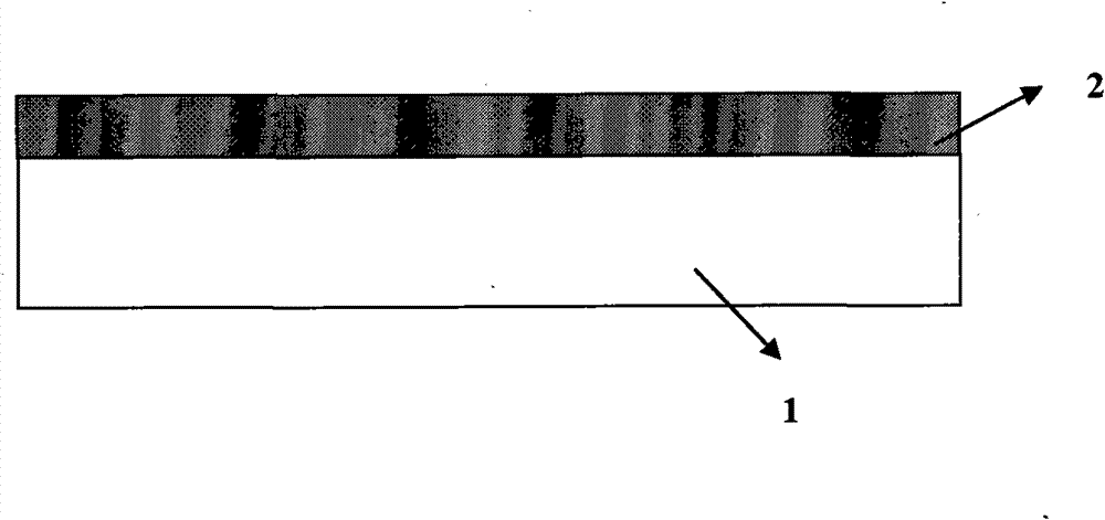
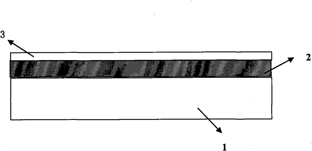
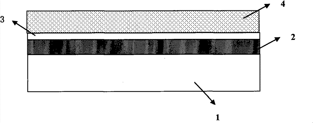
[0016] The invention is a method for adjusting Vtp (writing voltage) and Vte (inserting voltage) by using selective epitaxial doping instead of ion implantation, thereby improving the reliability of SONOS flash memory devices. Since the SONOS flash memory device needs to adjust the insertion and writing voltage to obtain the largest process window, it is usually necessary to perform ion implantation doping on the channel. However, ion implantation will cause damage to the silicon surface, thereby causing more defects at the interface between the tunneling oxide layer of SONOS and silicon, and ultimately directly reducing the reliability life of the device. At the same time, during the subsequent formation process of the tunnel oxide layer, ion implantation doping may be redistributed, increasing the instability of device performance. The pres...
PUM
 Abstract
Description
Claims
Application Information