Preset cavity type SOI (silicon on insulator) substrate film bulk acoustic wave filter and manufacturing method thereof

A thin-film bulk acoustic wave and manufacturing method technology, applied to electrical components, impedance networks, etc., can solve the problems of increasing the process, the impact of structural reliability, and the long time required for release, and achieve the effect of simple process and easy integration

Active Publication Date: 2011-07-13
CHINA ELECTRONICS TECH GRP NO 26 RES INST
View PDF10 Cites 24 Cited by
  • Summary
  • Abstract
  • Description
  • Claims
  • Application Information

AI Technical Summary

Problems solved by technology

The FBAF products produced by Fujitsu have the following difficulties: (1) The cavity-backed FBAR needs to be carved through the entire thickness of the silicon wafer, which has a certain impact on the structural reliability; (3) During the release process of the sacrificial layer, the surroundings of the sacrificial layer, especially the upper and lower surfaces, are all surrounded by electrodes and silicon wafers, and it takes a long time t...

Method used


Image

  • Preset cavity type SOI (silicon on insulator) substrate film bulk acoustic wave filter and manufacturing method thereof
  • Preset cavity type SOI (silicon on insulator) substrate film bulk acoustic wave filter and manufacturing method thereof
  • Preset cavity type SOI (silicon on insulator) substrate film bulk acoustic wave filter and manufacturing method thereof

Examples


Embodiment Construction

[0052] The preferred embodiments of the present invention will be described in detail below in conjunction with the accompanying drawings; it should be understood that the preferred embodiments are only for illustrating the present invention, rather than limiting the protection scope of the present invention.

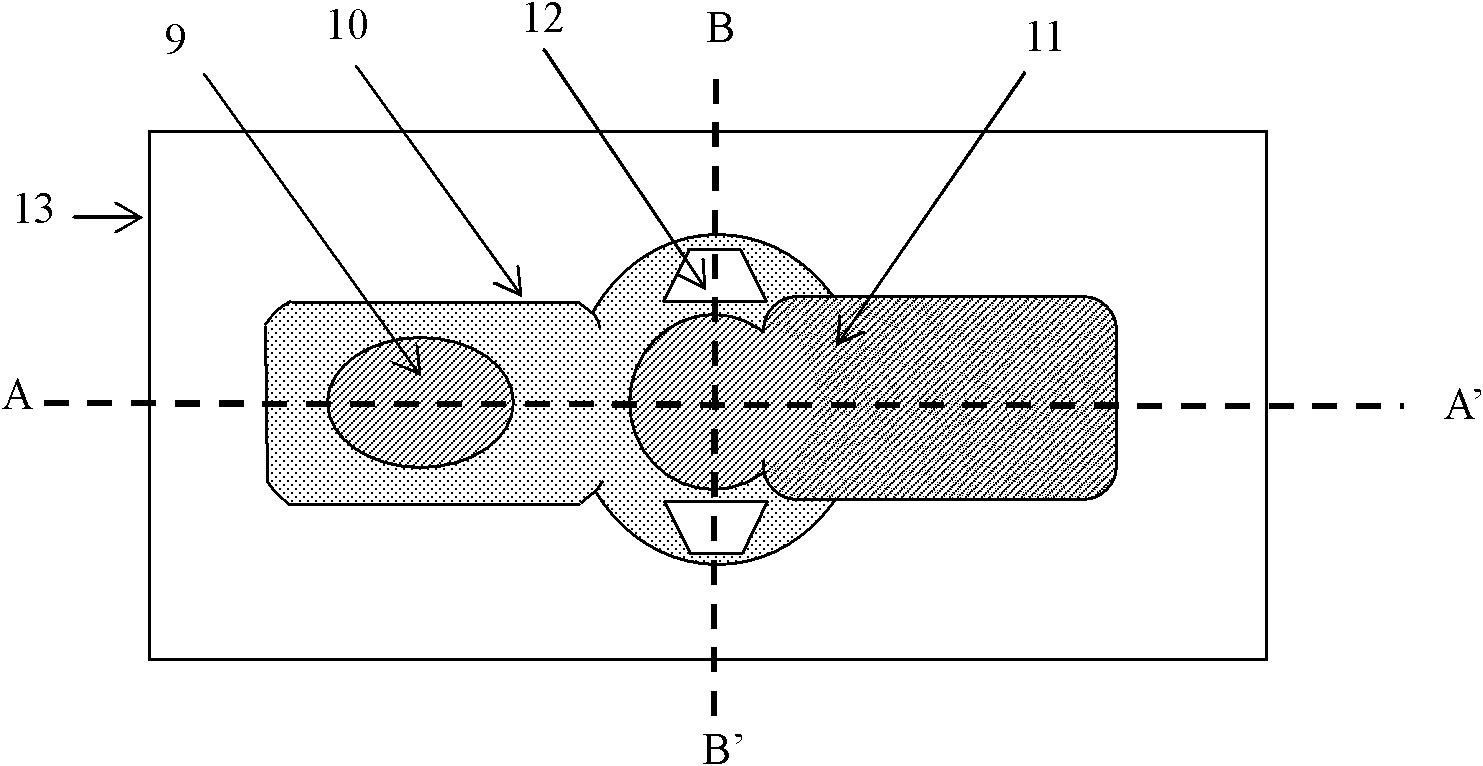
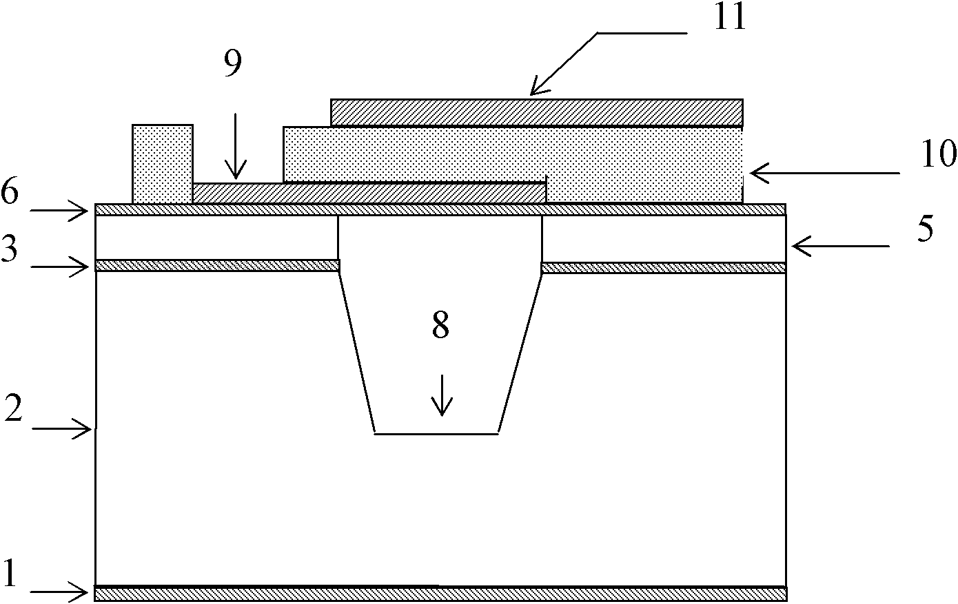
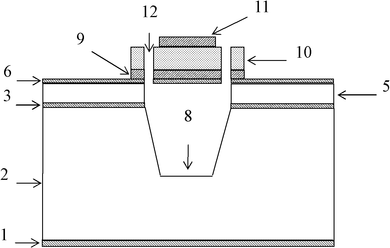
[0053] figure 1 It is the top plan view of the FBAR unit of the present invention, figure 2 for the invention figure 1 Middle A-A' profile, image 3 for the invention figure 1 In the sectional view of BB', as shown in the figure, the preset cavity-type SOI substrate thin-film bulk acoustic wave filter provided by the present invention includes a plurality of thin-film bulk acoustic wave resonators connected by electrical cascading, each thin-film bulk acoustic wave filter The acoustic wave resonator includes a preset cavity 8 type SOI substrate 13 and a transducer arranged on the SOI substrate 13, the transducer includes a bottom electrode 9, a top electrode 11 and ...


PUM

PropertyMeasurementUnit
Depthaaaaaaaaaa
Thicknessaaaaaaaaaa
Thicknessaaaaaaaaaa

Abstract

The invention discloses a preset cavity type SOI (silicon on insulator) substrate film bulk acoustic wave filter and a manufacturing method thereof, relating to the field of electronic devices. The filter is formed by electrically cascading a plurality of film bulk acoustic wave resonators which are manufactured on a preset cavity type SOI substrate, wherein each resonator comprises a piezoelectric film, a base electrode and a top electrode; a groove is arranged on the upper surface of substrate silicon of the SOI substrate; a sealed cavity is formed by the substrate silicon having the groove and top silicon; the top silicon is transferred from a groove-free SOI substrate by using a bonding technique and has even and controllable thickness; the cascaded mode of the filter includes a balancing bridge type, a stair type and a grid type; the frequency of the filter is adjustable and can be adjusted by controlling the thickness by controlling the etching time of the top silicon above the cavity; the electrodes of the resonators are approximate to oval, which is beneficial to the enhancement of the energy trap action; and a duplexer and a multiplexer can be formed by using the filter. In the invention, the advantages of SOI material are taken, the relative technique of a sacrifice layer is unnecessary, the process is simple, and the filter and the manufacturing method thereof are suitable for batch production.

Description

technical field [0001] The invention relates to the field of microelectronic devices, in particular to a thin-film bulk acoustic wave filter. Background technique [0002] Film bulk acoustic wave filter (FBAF) is a device that uses acoustic resonance to achieve electrical frequency selection. The common structure of FBAF is composed of several film bulk acoustic resonator (FBAR) units that are electrically cascaded. The basic working principle of FBAR is: when an electrical signal is loaded on the FBAR, the piezoelectric film in the device converts the electrical signal into an acoustic signal through the inverse piezoelectric effect, and the specific acoustic structure of the device presents selectivity to acoustic signals of different frequencies , to achieve the function of frequency regulation. [0003] The rapid development of wireless communication technology (such as mobile communication, wireless sensor network) and radar technology requires more and more high-perfo...

Claims


Application Information

Patent Timeline
IPC IPC(8): H03H9/54H03H3/02
Inventor 杨增涛马晋毅欧黎冷俊林杨正兵赵建华陈运祥周勇陈小兵傅金桥张龙张涛曹亮
Owner CHINA ELECTRONICS TECH GRP NO 26 RES INST
Why Eureka
Try Eureka