Embedded strong-current high-power PCB (Printed Circuit Board) and manufacturing method thereof

A technology of PCB board and manufacturing method, applied in the field of PCB board manufacturing, can solve the problems of large space occupation, high cost, complicated assembly process, etc.

Active Publication Date: 2011-07-13
BOMIN ELECTRONICS CO LTD
View PDF4 Cites 34 Cited by
  • Summary
  • Abstract
  • Description
  • Claims
  • Application Information

AI Technical Summary

Problems solved by technology

[0006] In view of this, the object of the present invention is to provide an embedded high-current high-power PCB board and its manufacturing method to solve the complex assembly process, complex assem

Method used


Image

  • Embedded strong-current high-power PCB (Printed Circuit Board) and manufacturing method thereof
  • Embedded strong-current high-power PCB (Printed Circuit Board) and manufacturing method thereof
  • Embedded strong-current high-power PCB (Printed Circuit Board) and manufacturing method thereof

Examples


Embodiment Construction
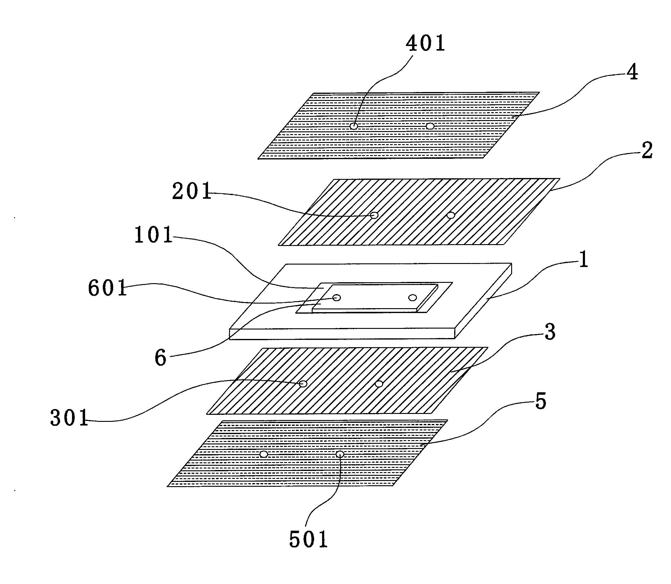
[0031] The core idea of ​​the present invention is: the present invention embeds a conductor structure in the core board of the PCB board, realizes the interconnection between the large current output end and the instrument input end through the conductor structure, and can make the conductor structure and the PCB board Its own circuit design connection to realize the circuit and power control of the instrument.

[0032] In order to illustrate the idea and purpose of the present invention, the present invention will be further described below in conjunction with the accompanying drawings and specific embodiments.

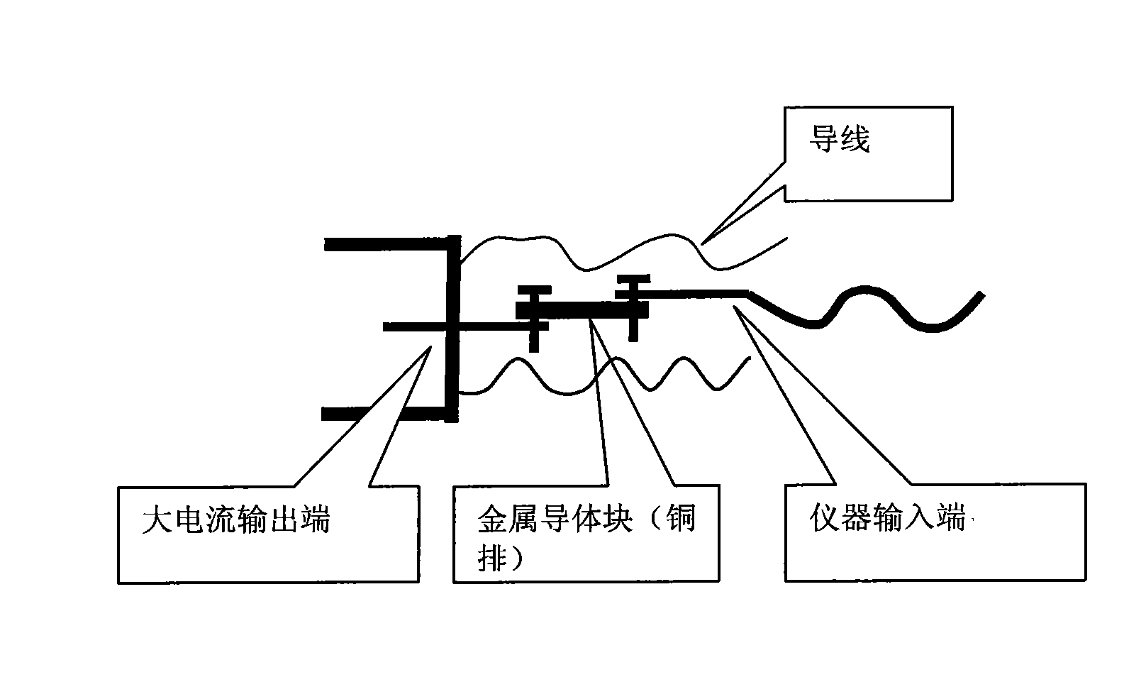
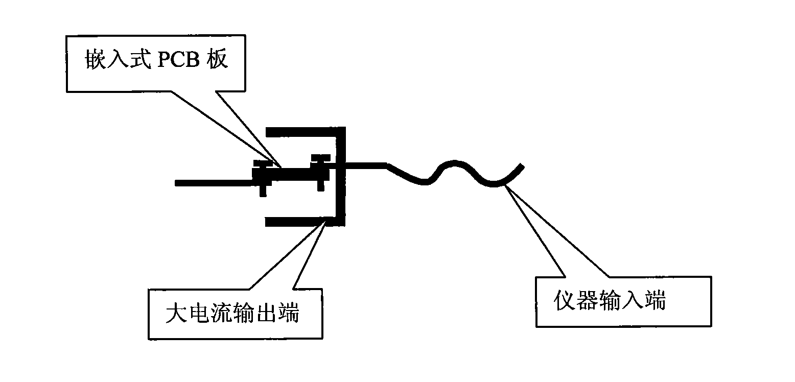
[0033] See figure 2 as shown, figure 2 It is a schematic diagram of the connection between the current output end of the high-current high-power electronic product of the present invention and the instrument input end through an embedded high-current high-power PCB board. Among them, the current output terminal of the current high-current and high-power electron...


PUM


Abstract

The invention discloses an embedded strong-current high-power PCB (Printed Circuit Board) and a manufacturing method thereof. The method comprises: (1) milling a hollow groove on a core board; (2) fixedly clamping and embedding a conductor structure member which is same as the hollow groove in shape and not larger than the core board into thickness in the hollow groove; (3) laminating a first copper foil layer on the upper surface of the core board by a first semicuring piece, and laminating a second copper foil layer on the lower surface of the core board by a second semicuring piece; (4) drilling the laminated product, performing image transfer and image making on the first and second copper foil layers, forming a circuit needed by design and a part meeting large power and circuit control on the copper foil layers, simultaneously, performing hole metallization on the formed through hole to obtain the thickness of copper needed on the hole wall, and then performing solder masking manufacture; and (5) performing blind-sink hollowing on corresponding parts, needing to be connected on the product, of the conductor structure member after solder masking, exposing the conductor structure member, drilling the conductor structure member to form wire holes connected with other external connecting pieces. Compared with the prior art, in the invention, the conductor structure member is embedded into the inner layer of the PCB, interconnection of a large-current output end and an instrument input end by utilizing holes or surfaces on the conductor structure member, simultaneously, component packaging is performed by other circuit part lines except the high-power conductor structure member embedded into the PCB so as to control the circuit, so that the original wire connection is replaced to achieve the circuit control part, and the problems in the integration process of the power and circuit control parts of strong-current high-power electronic products are solved.

Description

technical field [0001] The invention belongs to the technical field of PCB board manufacturing, in particular to an embedded high-current high-power PCB board and a manufacturing method thereof, which are mainly used for the integration of power parts and control parts of high-current high-power electronic products. Background technique [0002] Printed Circuit Board (Printed Circuit Board) referred to as PCB, also known as printed board, is one of the important components of electronic products. Electronic products made of printed circuit boards have the advantages of high reliability, good consistency, high mechanical strength, light weight, small size, and easy standardization. Almost every kind of electronic equipment, ranging from electronic watches and calculators to large computers, communication equipment, and electronic radar systems, as long as there are electronic components, the electrical interconnection between them will use printed boards. [0003] In the ear...

Claims


Application Information

Patent Timeline
IPC IPC(8): H05K1/02H05K3/00
Inventor 黄建国郭阳陆景富
Owner BOMIN ELECTRONICS CO LTD
Why Eureka
Try Eureka