

Power field-effect tube and method for manufacturing same
A technology of power field effect transistors and manufacturing methods, which is applied in semiconductor/solid-state device manufacturing, electrical components, circuits, etc., and can solve problems such as product scrapping, aspect ratio limitations, and affecting device performance
- Summary
- Abstract
- Description
- Claims
- Application Information
AI Technical Summary
Problems solved by technology
Method used
Image

Examples
Embodiment Construction
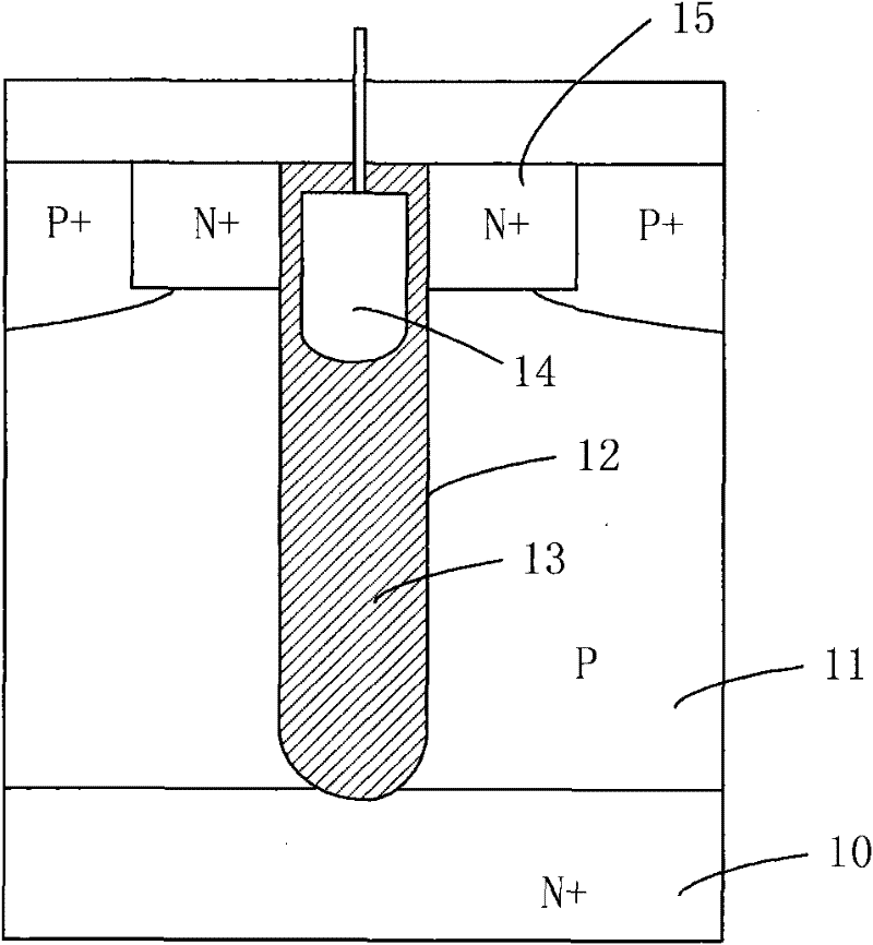
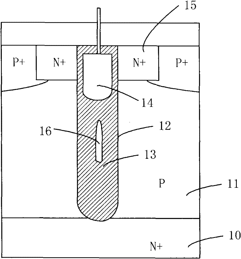
[0017] The invention aims to provide an improved power field effect transistor and a manufacturing method thereof, so that the gate trenches can be filled more easily, the aspect ratio of the gate trenches can be enlarged, and the performance of the device can be improved.
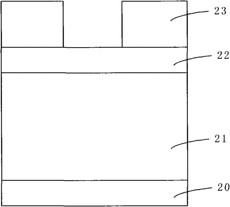
[0018] A method for manufacturing a power field effect transistor, comprising the steps of: (a) providing a substrate, forming an inversion substrate on the substrate, and forming a first mask layer with a first opening on the inversion substrate; (b) Using the first mask layer as a mask, etching a part of the inversion substrate to form a first trench; (c) depositing a second mask layer in the first trench and on the sidewall of the first opening, and etching back The second mask layer, so that the second mask layer has a second opening, and the width of the second opening is smaller than the first opening; (d) using the second mask layer as a mask, etching the reverse type substrate, in the reverse type ...
PUM
 Abstract
Description
Claims
Application Information