Method for preparing large-size silicon pore array

A large-size, silicon-hole technology, applied in the field of preparing large-size silicon-hole arrays, can solve the problems of high manufacturing cost and difficulty of large-size silicon-hole arrays

Active Publication Date: 2012-08-29
INST OF ELECTRICAL ENG CHINESE ACAD OF SCI
View PDF3 Cites 4 Cited by
  • Summary
  • Abstract
  • Description
  • Claims
  • Application Information

AI Technical Summary

Problems solved by technology

[0007] The purpose of the present invention is to overcome the disadvantages of difficulty and high preparation cost of preparing large-scale silicon hole arrays on p-type silicon substrates with low resistivity in the prior art, and propose a method of using metal particles to assist silicon substrates to anode Oxidation etching method

Method used


Image

  • Method for preparing large-size silicon pore array
  • Method for preparing large-size silicon pore array
  • Method for preparing large-size silicon pore array

Examples


Embodiment 1

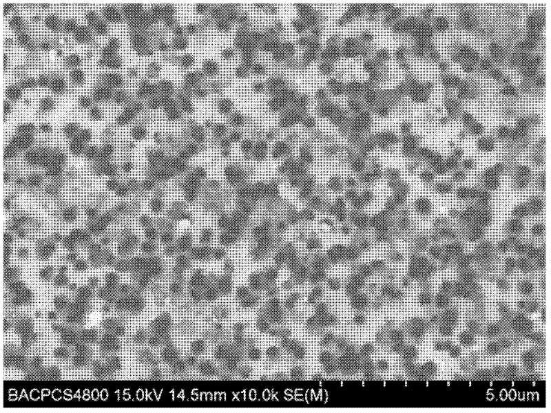
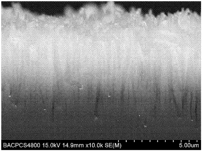
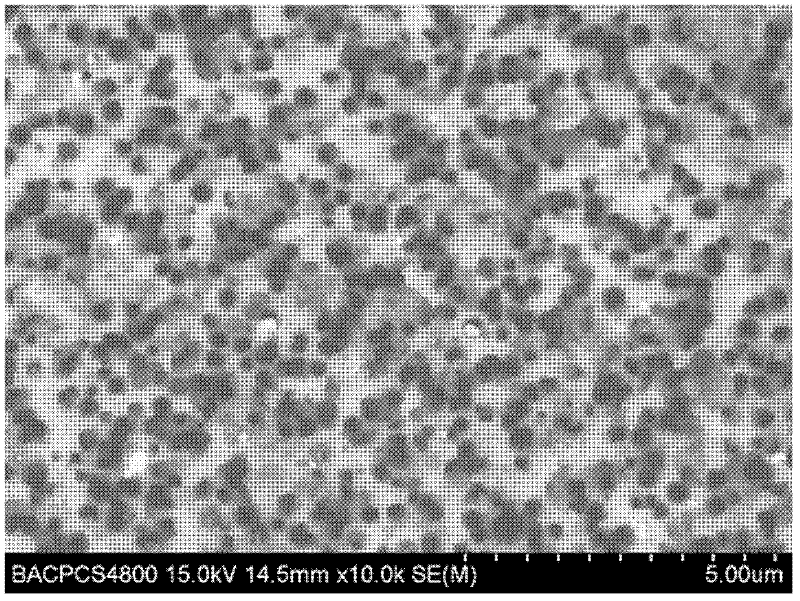
[0019] First, immerse a p-type silicon substrate with a resistivity of about 0.5Ω·cm into HF: AgNO 3 In the mixed aqueous solution, silver nanoparticles are deposited on the surface of the p-type silicon substrate. The HF: AgNO 3 In the mixed solution, the concentration of HF is 0.07M, AgNO 3 The concentration is 1×10 -3 M, the immersion time of the silicon substrate is 1 minute. Then the silicon substrate deposited with silver nanoparticles was immersed in HF:H 2 O 2 : H 2 Anodizing in O mixed solution, the HF:H 2 O 2 : H 2 The ratio of O mixture is 45:150:360 by volume, and the current density for anodizing is 0.06A / cm 2 , The corrosion time is 30 minutes. figure 1 with figure 2 The scanning electron microscope (SEM) photographs of the surface and cross-section of the silicon hole array prepared according to this embodiment are given. It can be seen that the diameter of the silicon hole array is about 200 nanometers and the depth is about 4 microns.


PUM

PropertyMeasurementUnit
electrical resistivityaaaaaaaaaa
diameteraaaaaaaaaa
diameteraaaaaaaaaa

Abstract

The invention discloses a method for preparing a large-size silicon pore array. The method comprises the steps as follows: firstly, selecting a p-type silicon substrate with low resistance rate, and depositing metal particles; secondly, carrying out anodic oxidation on the silicon substrate with the metal particles deposited on the surface in an oxidant-containing solution; and thirdly, obtaining the large-size silicon pore array of nanometer to micron dimension by controlling current density and corrosion time under constant current.

Description

Technical field [0001] The invention relates to the field of semiconductors, in particular to a method for preparing large-size silicon hole arrays. Background technique [0002] The low-dimensional micro-nano structure is currently the research frontier in the field of microelectronics and optoelectronics. The reduction in the size of the micro-nano structure and the mesoscopic physical effects can bring about a substantial increase in the integration and performance of the device. In traditional planar solar cells, in order to achieve complete light absorption, the thickness of the absorption region requires 100 microns for Si and 1-3 microns for GaAs. The photogenerated carriers need long enough life to be transported through this thickness. Therefore, the material in the absorption zone is required to have high purity. If low-dimensional micro-nano structures, such as nanowires, nanorods, and other materials are used as the absorption region, the light absorption and the co...

Claims


Application Information

Patent Timeline
Patent Type & Authority Applications(China)
IPC IPC(8): C25D11/32C25D15/00C25F3/12C25F3/14B81C1/00
Inventor 赵雷李兆辰王文静
Owner INST OF ELECTRICAL ENG CHINESE ACAD OF SCI
Why Eureka
Try Eureka