Radiation detector

A radiation detector and detector technology, applied in radiation control devices, semiconductor devices, discharge tubes, etc., can solve the problems of increasing material thickness

Active Publication Date: 2011-07-20
FEI CO
View PDF4 Cites 14 Cited by
  • Summary
  • Abstract
  • Description
  • Claims
  • Application Information

AI Technical Summary

Problems solved by technology

[0023] Although when detecting photons with short wavelengths SiO 2 A protective layer is acceptable (due to SiO 2 high transparency for these photons), but the addition of a protective layer increases the thickness of the material that electrons have to traverse before entering the depletion region

Method used


Image

  • Radiation detector
  • Radiation detector
  • Radiation detector

Examples


Embodiment Construction

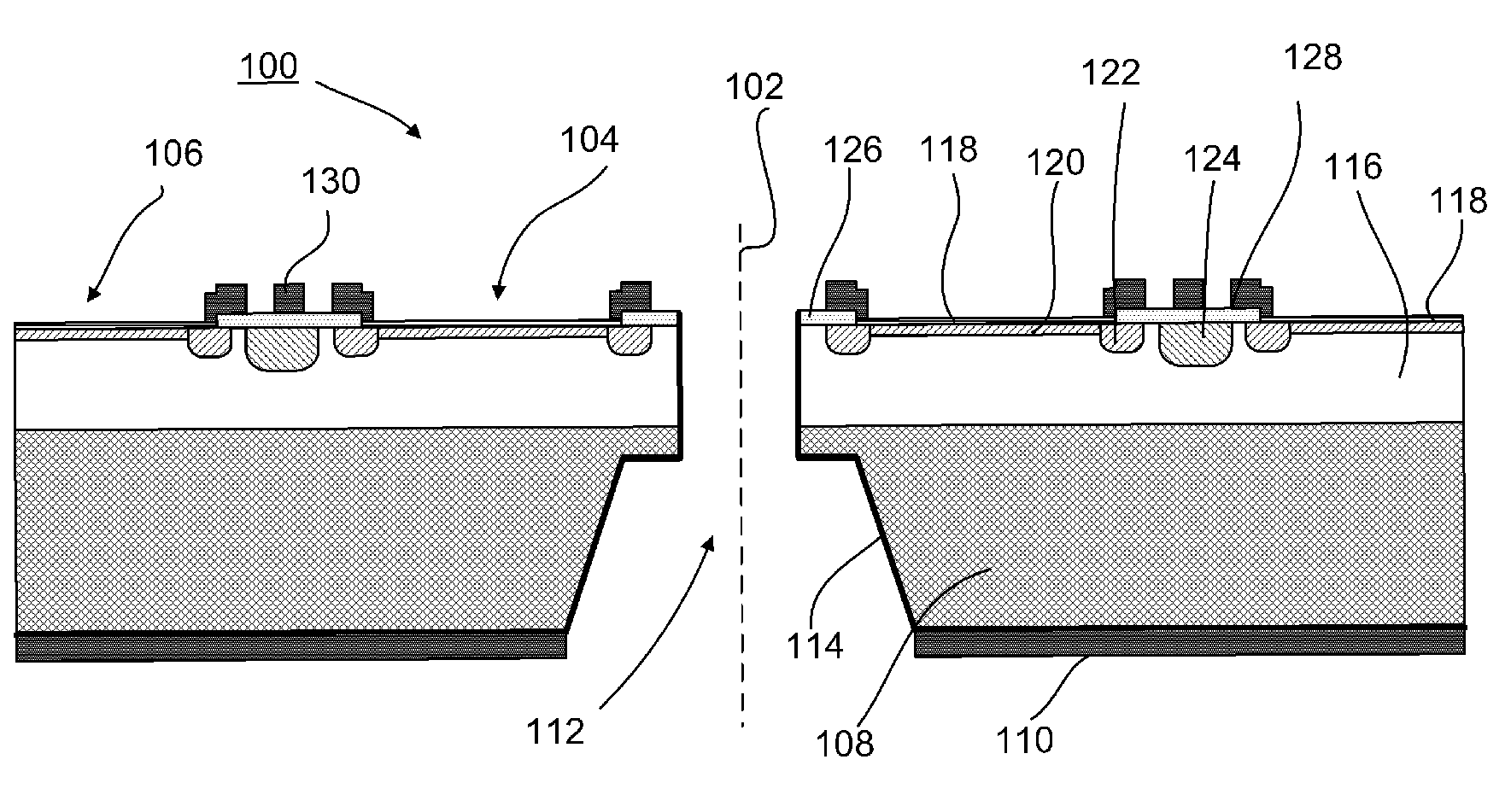
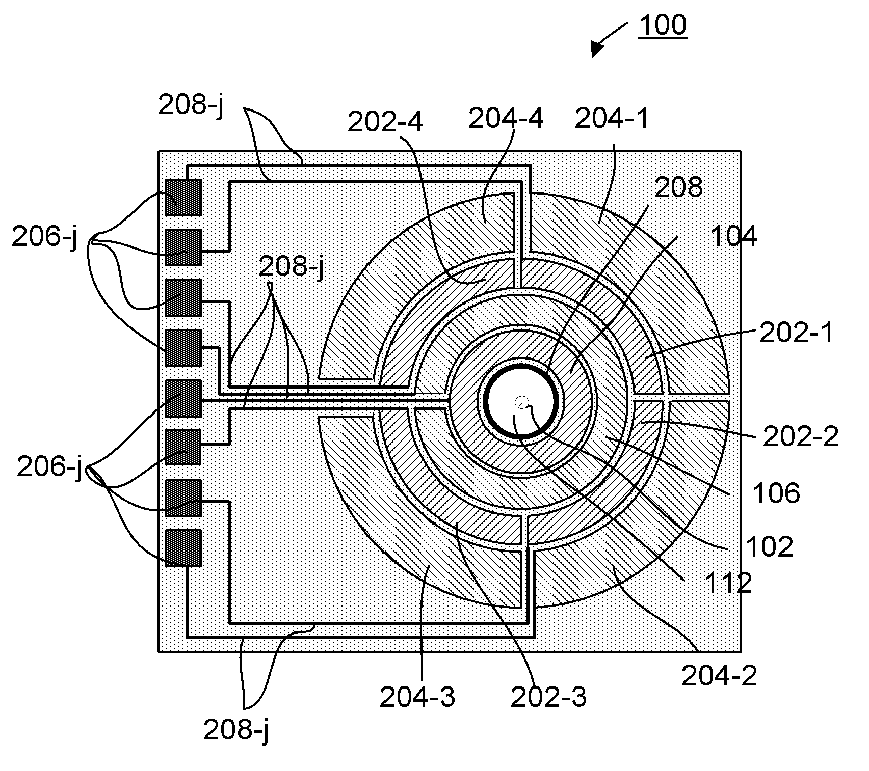
[0078] figure 1 A cross-section of a sensor including a plurality of detectors according to the present invention is schematically shown.

[0079] It shows the sensor 100, which is shown symmetrical about the axis 102. The sensor shows two detectors 104 and 106, each having an area sensitive to radiation. The detector can be a ring detector, but each ring can be further divided into segments, such as three 120° segments, or four 90° segments, each of which forms a separate detector.

[0080] The sensor includes an n-type substrate 108 that is metalized on one side, thereby forming a back electrode 110. On the other side of the substrate, an intrinsic layer in the form of an epitaxial layer 116 is formed to have a thickness of, for example, 40 μm. On top of the epitaxial layer, the boron layer 118 is deposited, thereby forming the p of the silicon boride layer 120 + Type diffusion layer. Around the radiation-sensitive area, a p-doped (boron-doped) boundary 122 is formed. The de...


PUM


Abstract

The invention discloses a process for manufacturing a radiation detector for detecting e.g. 200 eV electrons. This makes the detector suited for e.g. use in an Scanning Electron Microscope. The detector is a PIN photodiode with a thin layer of pure boron connected to the p+-diffusion layer. The boron layer is connected to an electrode with an aluminium grid to form a path of low electrical resistance between each given point of the boron layer and the electrode. The invention addresses forming the aluminium grid on the boron layer without damaging the boron layer. To that end the grid of aluminium is formed by covering the boron layer completely with a layer of aluminium and then removing part of the layer of aluminium by etching, the etching comprising a first step (304) of dry etching, the step of dry etching defining the grid but leaving a thin layer of aluminium on the part of the boron layer to be exposed, followed by a second step (308) of wet etching, the step of wet etching completely removing the aluminium from the part of the boron layer to be exposed.

Description

Technical field [0001] The present invention relates to a method of manufacturing a radiation detector with a radiation-sensitive surface. The method includes the following steps: [0002] · A step of providing a planar substrate, the substrate showing an n-doped plane and an intrinsic layer formed on the n-doped plane; [0003] · The step of depositing a layer including boron on the intrinsic layer, thereby forming a p+ type diffusion layer and a top layer including boron; [0004] · The step of forming a grid of conductive material on the boron, at least a part of the grid is formed on the top layer, the grid is electrically connected to the top layer, and a part of the top layer Exposed, the grid forms a first electrode; and [0005] · The step of forming a second electrode connected to the n-doped plane. [0006] Such a radiation detector is known from European Patent Application No. EP2009705. Background technique [0007] In a particle optical device, a beam of particles (such as...

Claims


Application Information

Patent Timeline
Patent Type & Authority Applications(China)
IPC IPC(8): H01L31/18H01L31/0224H01L27/144H01L31/115
CPCH01J37/244H01L31/105H01L31/022408H01L31/1185
Inventor G.N.A.范维恩C.S.库伊曼L.K.南弗T.L.M.肖尔特斯A.萨基克
Owner FEI CO
Why Eureka
Try Eureka