
Time-delay circuit

A delay circuit and circuit technology, applied in the direction of electrical components, pulse processing, single output arrangement, etc., can solve the problems of large deviation and low delay accuracy, and achieve the effect of improving yield and accurate delay

Inactive Publication Date: 2011-07-20
SHANGHAI HUAHONG GRACE SEMICON MFG CORP
View PDF3 Cites 22 Cited by
  • Summary
  • Abstract
  • Description
  • Claims
  • Application Information

AI Technical Summary

Problems solved by technology

Therefore, the delay produced by the traditional delay circuit has a relatively large deviation under different conditions, and the delay accuracy is not high.

Method used


Image

  • Time-delay circuit
  • Time-delay circuit
  • Time-delay circuit

Examples


Embodiment Construction

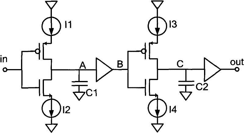
[0017] An embodiment of the delay circuit of the present invention is as image 3 As shown, it includes a first PMOS transistor M1 of a P-type transistor, a second NMOS transistor M2 of an N-type transistor, a third PMOS transistor M3 of a P-type transistor, a fourth NMOS transistor M4 of an N-type transistor, a first buffer, a second buffer, The first capacitor C1, the second capacitor C2, the first current source circuit, the second current source circuit, the third current source circuit, and the fourth current source circuit;

[0018] The gates of the first PMOS transistor M1 and the second NMOS transistor M2 are short-circuited for connecting to the input signal terminal in, the drain of the first PMOS transistor M1 is short-circuited with the source of the second NMOS transistor M2 and connected to the first buffer The input terminal A of the device M1 and one end of the first capacitor C1, the source of the first PMOS transistor M1 is connected to the power supply volta...


PUM


Abstract

The invention discloses a time-delay circuit. In the invention, a first PMOS (P-channel Metal Oxide Semiconductor) tube, a second NMOS (N-channel metal oxide semiconductor) tube, a first current source circuit, a second power supply circuit and a first capacitor form a first capacitance charge and discharge switching circuit; a third PMOS tube, a fourth NMOS tube, a third current source circuit, a fourth current source circuit and a second capacitor form a second capacitance charge and discharge switching circuit; and an input signal is output sequentially through the first capacitance charge and discharge switching circuit, a first buffer, the second capacitance charge and discharge switching circuit and a second buffer or a phase inverter. The time-delay circuit eliminates the influence of process offsets by utilizing the time delay of the two capacitance charge and discharge switching circuits to mutually compensate so as to ensure that the time delay is more precise.

Description

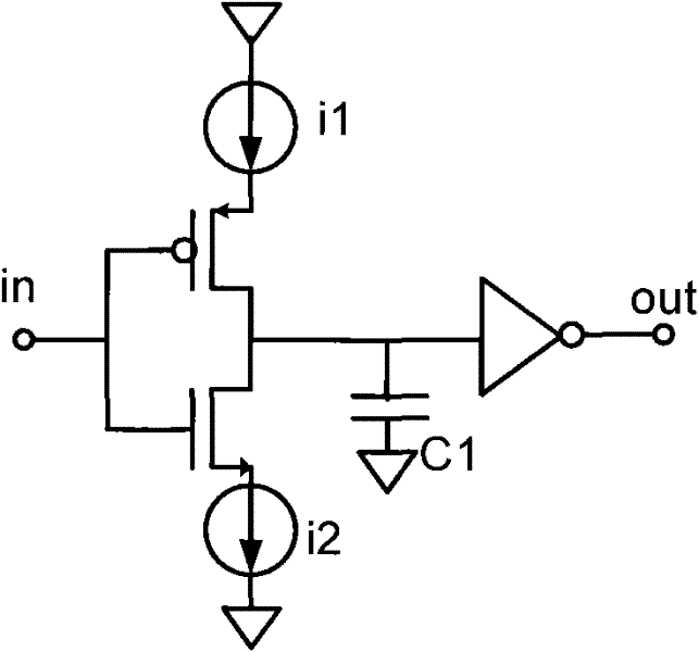
technical field [0001] The invention relates to a semiconductor integrated circuit, in particular to a delay circuit. Background technique [0002] Delay circuits are widely used in many integrated circuit IP (Intellectual Property). Accurate delay circuits can improve the performance of integrated circuit IP and increase the yield of wafers, especially in NVM (Non-Volatile Memory non-volatile In the field of volatile memory), a precise delay circuit can improve the reading speed of NVM. [0003] The traditional delay circuit is to directly use the delay accumulation of the inverter to generate the required delay (such as figure 1 shown), or use the reference current source to charge and discharge the capacitor with the required delay (such as figure 2 shown). Since the flipping voltage of a buffer or inverter is greatly affected by supply voltage and process variation), the figure 1 The delay circuit shown is sensitive to process variation, while the figure 2 The del...

Claims


Application Information

Patent Timeline
Patent Type & Authority Applications(China)
IPC IPC(8): H03K5/13H03K5/134
Inventor 冯国友
Owner SHANGHAI HUAHONG GRACE SEMICON MFG CORP
Learn More