Shift register circuit, display device and shift register circuit driving method

A shift register and circuit technology, applied in static memory, digital memory information, instruments, etc., can solve problems such as large overvoltage of transistor T5, and achieve the effect of improving reliability

Inactive Publication Date: 2011-07-20
SHARP KK
View PDF4 Cites 7 Cited by
  • Summary
  • Abstract
  • Description
  • Claims
  • Application Information

AI Technical Summary

Problems solved by technology

As a result, the transistor T5 is turned on, and the clock signal input from the clock input terminal CKA appears at the source of the transistor T5, but at the moment when the clock pulse (high level) i

Method used


Image

  • Shift register circuit, display device and shift register circuit driving method
  • Shift register circuit, display device and shift register circuit driving method
  • Shift register circuit, display device and shift register circuit driving method

Examples


Embodiment Construction

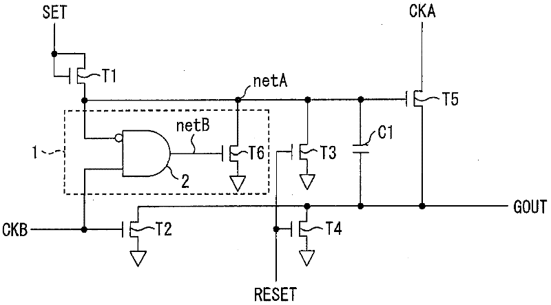
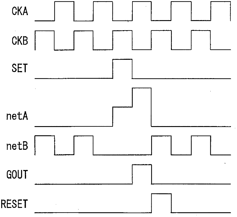
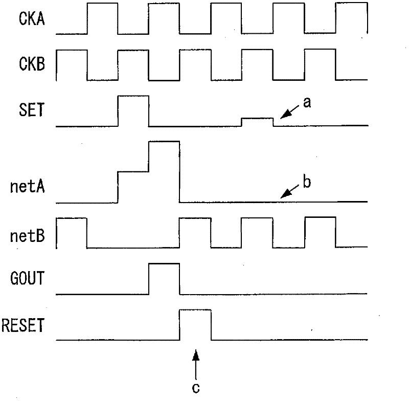
[0100] according to Figure 1 to Figure 11 One embodiment of the present invention will be described below.

[0101] Figure 11 The configuration of a liquid crystal display device 11 as a display device of the present embodiment is shown.

[0102] The liquid crystal display device 11 includes a display panel 12 , a flexible printed circuit board 13 , and a control board 14 .

[0103] The display panel 12 is made of amorphous silicon on a glass substrate to form a display area 12a, a plurality of gate lines (scanning signal lines) GL..., a plurality of source lines (data signal lines) SL... and gate drivers (scanning signal lines) line drive circuit) 15 active matrix type display panel. The display panel 12 can also be made of polycrystalline silicon, CG silicon, microcrystalline silicon, or the like. The display area 12a is an area where a plurality of pixels PIX... are arranged in a matrix. The pixel PIX includes a TFT 21 as a pixel selection element, a liquid crystal c...


PUM


Abstract

A control part (1) generates a control signal, which puts a first switching element (T6) in a conducting state, from the non-active electric potential level of a charging node (netA) at a charging node (netA) and the active electric potential level of a second clock signal in an active period of a second clock signal, and outputs to a control terminal (netB) for conduction and blocking of the first switching element (T6).

Description

technical field [0001] The present invention relates to a shift register circuit made monolithically in a display panel. Background technique [0002] In recent years, gate monolithic circuits have been developed in which costs are reduced by forming gate drivers on liquid crystal panels using amorphous silicon. The gate monolithic circuit is also called no gate driver, panel built-in gate driver, panel inner gate (gate in panel), etc. [0003] Figure 12 A configuration example of a shift register circuit constituting a gate driver formed by a gate monolithic circuit is shown. [0004] In this shift register circuit, each stage (shift register stage) SRk (k is a natural number) has: a set terminal SET, an output terminal GOUT, a reset terminal RESET, a low-level power supply input terminal VSS and a clock input terminal CKA, CKB. In each stage of SRk (k≧2), the output signal GOUT of the preceding stage SRk-1 is input to the set terminal SET (substituted by an output term...

Claims


Application Information

Patent Timeline
IPC IPC(8): G11C19/28G09G3/20G09G3/36G11C19/00
CPCG11C19/28G09G3/3677G11C19/184G09G2310/0286
Inventor 岩本明久水永隆行森井秀树太田裕己生田庆
Owner SHARP KK
Why Eureka
Try Eureka