Enhanced wire bond stability on reactive metal surfaces of a semiconductor device by encapsulation of the bond structure

A technology of bonding wires and semiconductor tubes, applied in semiconductor devices, semiconductor/solid-state device manufacturing, semiconductor/solid-state device components, etc., can solve problems such as increased manufacturing costs, complex processing procedures, and increased cycle time

Inactive Publication Date: 2011-07-20
GLOBALFOUNDRIES INC
View PDF0 Cites 2 Cited by
  • Summary
  • Abstract
  • Description
  • Claims
  • Application Information

AI Technical Summary

Problems solved by technology

[0010] As a result, efficient wire bonding techniques can be used based on the aluminum layer 131 in the aforementioned known methods, however, complex processing procedures are required for depositing and patterning the barrier / adhesion layer 132 and the aluminum layer 131
Therefore, in a complex manufacturing environment, in addition to the equipment and materials required for the formation of complex copper-based metallization systems, it is necessary to provide individual components for depositing and patterning the aluminum layer 131 and the barrier / adhesion layer 132. resources, thus resulting in increased cycle time and thus increased manufacturing costs

Method used


Image

  • Enhanced wire bond stability on reactive metal surfaces of a semiconductor device by encapsulation of the bond structure
  • Enhanced wire bond stability on reactive metal surfaces of a semiconductor device by encapsulation of the bond structure
  • Enhanced wire bond stability on reactive metal surfaces of a semiconductor device by encapsulation of the bond structure

Examples


Embodiment Construction

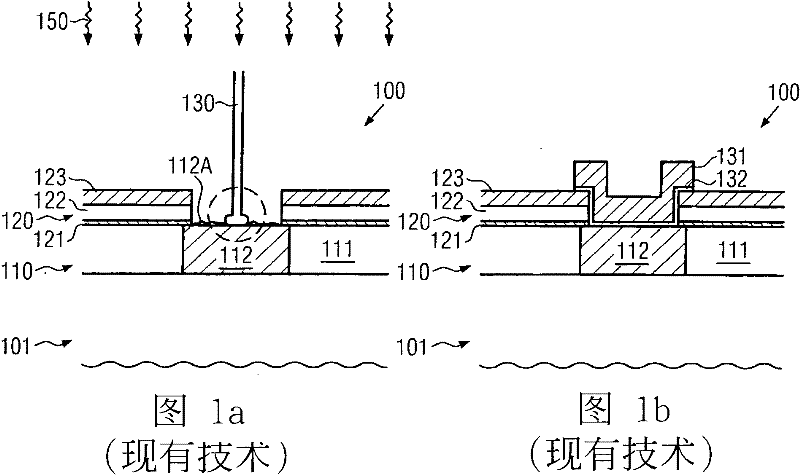
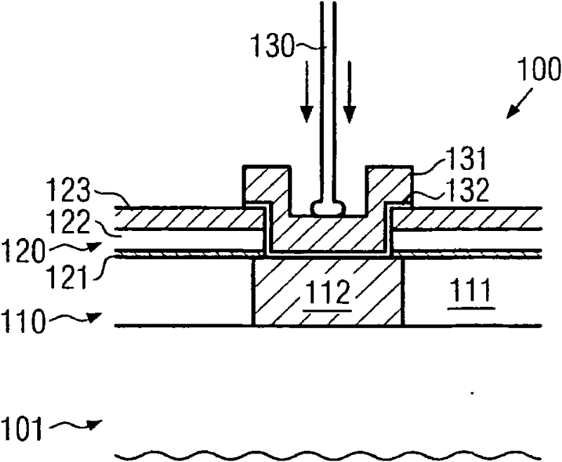
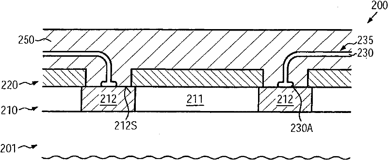
[0023] Various illustrative embodiments of the invention are described below. In the interest of brevity, not all features of an actual implementation are described in this specification. It will of course be appreciated that in the development of any such specific embodiment, many specific implementation decisions must be made to achieve the inventor's specific goals, such as conforming to system-related and business-related constraints that vary from embodiment to embodiment. Moreover, such a developmental effort would be appreciated to be complex and time-consuming, but would nonetheless be a routine undertaking for those with ordinary skill in the art having the benefit of this disclosure.

[0024] The subject matter of the present invention will be described with reference to the accompanying drawings. Various structures, systems and devices are depicted in the drawings for purposes of illustration only so as not to obscure the present invention with details that would b...


PUM


Abstract

The wire bond structure of sophisticated metallization systems, for instance based on copper, may be provided without a terminal aluminum layer and without any passivation layers for exposed copper surfaces (212S) by providing a fill material (250) after the wire bonding process in order to encapsulate at least the sensitive metal surfaces (212S) and a portion of the bond wire (230). Hence, significant cost reduction, reduced cycle times and a reduction of the required process steps may be accomplished independently from the wire bond materials used. Thus, integrated circuits requiring a sophisticated metallization system may be connected by wire bonding to the corresponding package (260) or carrier substrate with a required degree of reliability based on a corresponding fill material (250) for encapsulating at least the sensitive metal surfaces (212S).

Description

technical field [0001] The present invention relates to the field of integrated circuits, and more particularly to backend circuit processing for wirebond structures in precision metallization structures including highly reactive metals such as copper, etc. Background technique [0002] The fabrication of integrated circuits involves many complex processing steps to form circuit elements, such as transistors, capacitors, resistors, etc., in and on suitable semiconductor materials. In recent years, tremendous progress has been made in increasing the bulk density and overall functionality of integrated circuits. These advances have been achieved by shrinking individual circuit elements down to the deep sub-micron range (shrinking critical dimensions such as the gate length of field effect transistors to 30nm or less in use today). Thus, millions of circuit elements can be provided in one die, where complex interconnection configurations must also be designed, where each circu...

Claims


Application Information

Patent Timeline
Patent Type & Authority Applications(China)
IPC IPC(8): H01L23/24H01L23/485H01L21/56H01L23/31H01L21/60
CPCH01L2224/48839H01L2924/04953H01L2224/48747H01L24/45H01L2224/05647H01L2224/48699H01L2224/48091H01L2224/8592H01L2224/85375H01L24/48H01L2924/14H01L2224/85205H01L2924/01005H01L2924/01013H01L2224/45144H01L2924/01022H01L2224/48095H01L2224/85201H01L2224/48739H01L2924/30105H01L2224/48247H01L2224/48639H01L2224/48647H01L2924/1532H01L2924/01068H01L2924/01015H01L24/85H01L2924/04941H01L2224/48463H01L2924/05042H01L2924/01327H01L2924/01047H01L2224/04042H01L2224/45124H01L2924/01006H01L2924/19041H01L24/05H01L2224/45147H01L2924/01079H01L2924/01073H01L2924/01014H01L2224/48847H01L2224/48599H01L2224/05639H01L2924/01082H01L2924/01007H01L2924/014H01L2924/01029H01L2924/19043H01L2924/01019H01L2924/01033H01L2924/00014H01L2924/3025H01L2224/48799H01L2924/01075H01L2224/02166H01L2224/451H01L2924/1306H01L2924/181H01L2924/351H01L2224/78H01L2924/00H01L2924/00015H01L2924/00012H01L23/24H01L23/31H01L23/485
Inventor A·迈尔斯M·莱尔F·屈兴迈斯特
Owner GLOBALFOUNDRIES INC
Why Eureka
Try Eureka