Array substrate, manufacturing method thereof and liquid crystal display

A technology of an array substrate and a manufacturing method, which is applied in the field of liquid crystal display, can solve the problems of reduced public voltage signal load, large delay of RC signal, affecting picture quality, etc., so as to reduce the delay of RC signal, reduce resistance, and improve picture quality. Effect

Active Publication Date: 2011-07-27
BOE TECH GRP CO LTD +1
View PDF8 Cites 59 Cited by
  • Summary
  • Abstract
  • Description
  • Claims
  • Application Information

AI Technical Summary

Problems solved by technology

[0006] The common electrode of HFFS or HAD-SDS has a slit, which has higher resistance than the tiled whole common electrode, and the delay of the RC signal of the c

Method used


Image

  • Array substrate, manufacturing method thereof and liquid crystal display
  • Array substrate, manufacturing method thereof and liquid crystal display
  • Array substrate, manufacturing method thereof and liquid crystal display

Examples


Embodiment 1

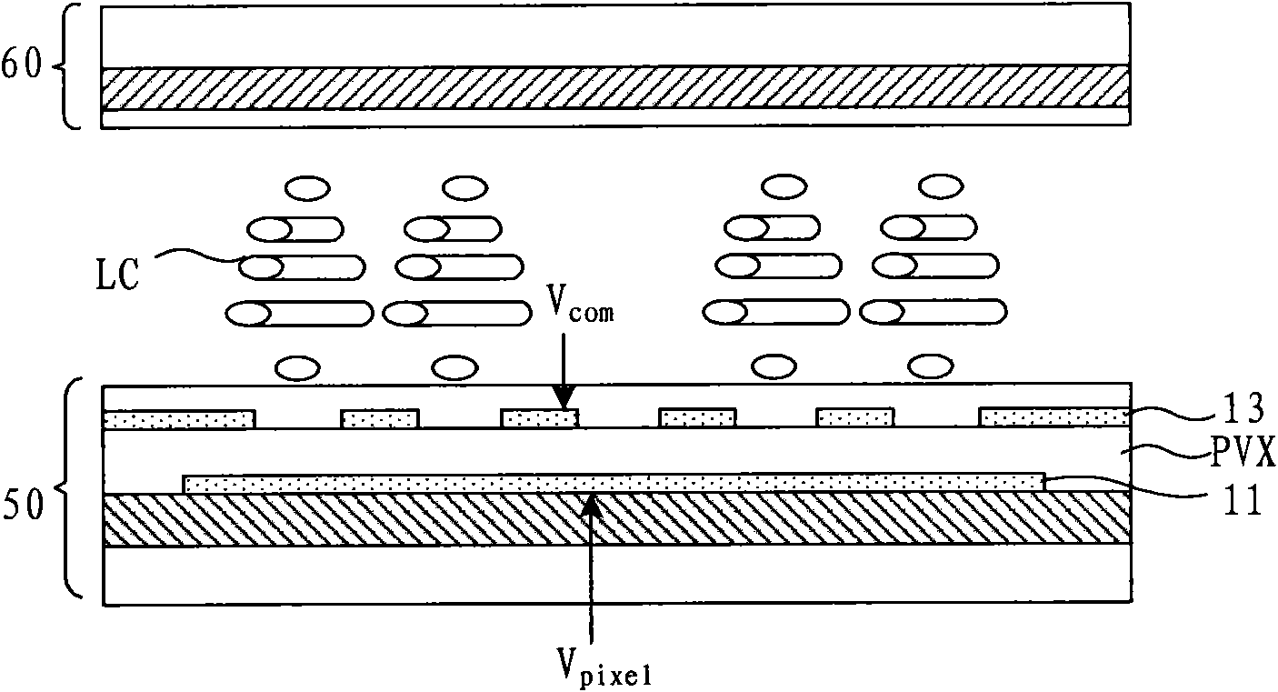
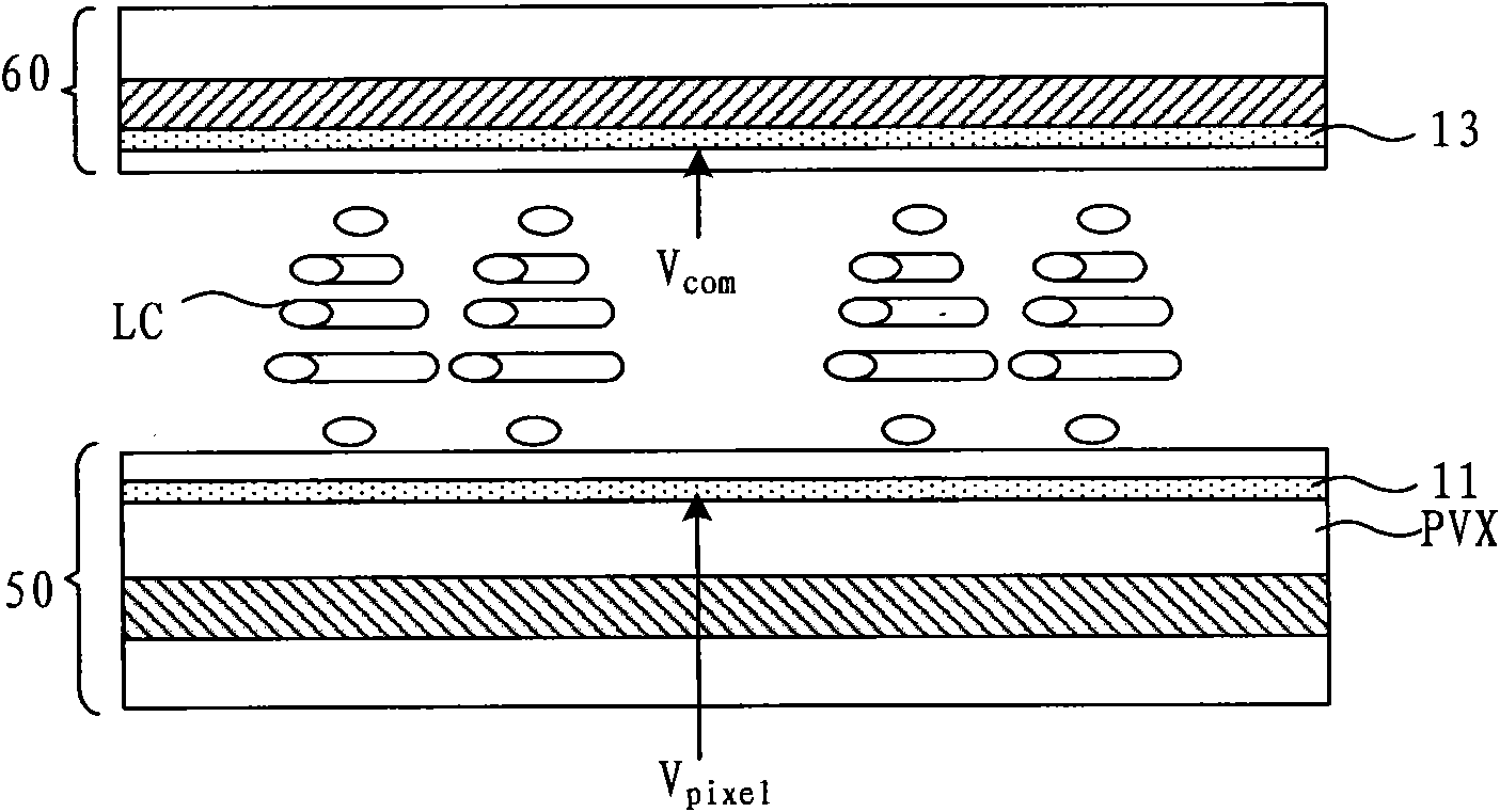
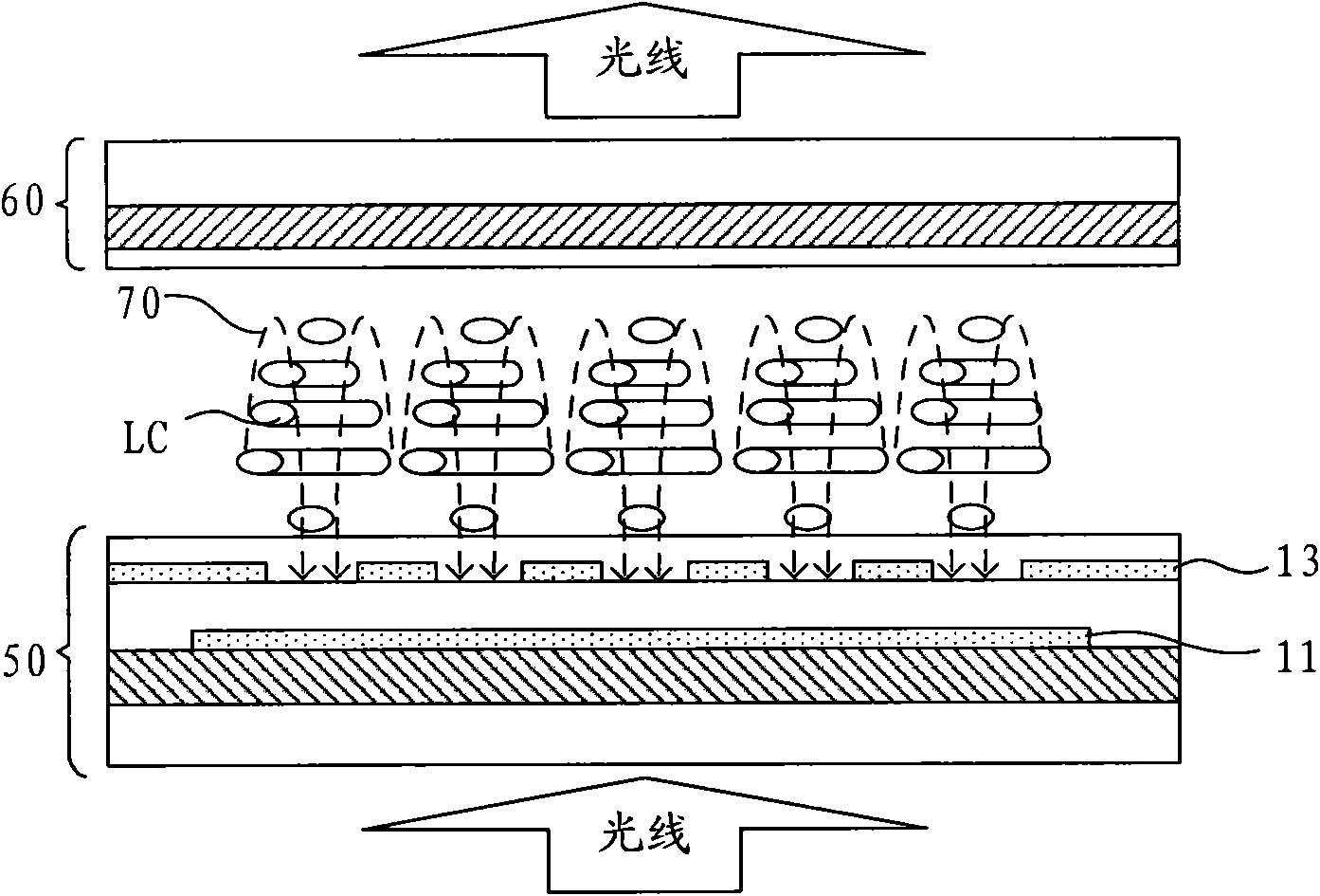
[0054] Figure 5 A schematic structural diagram of the array substrate provided in Embodiment 1 of the present invention, as shown in Figure 5 As shown, the array substrate includes a base substrate 1, and the pixel area 30 of the base substrate 1 is formed with data lines and gate lines that cross horizontally and vertically to form a plurality of pixel units, and each pixel unit includes a switching element, a pixel The electrode and the common electrode 13 , the common electrode 13 is an integral pattern with slits arranged in the pixel area, wherein: the common electrode line 12 is also formed in the pixel area 30 , and the common electrode line 12 communicates with the common electrode 13 .

[0055] In the array substrate of the liquid crystal display of HFFS or HAD-SDS mode, the common electrode line 12 can be formed in the pixel area 30, wherein, the common electrode line 12 and the common electrode 13 can be connected through contact via holes, and can also be directl...

Embodiment 2

[0058] The array substrate provided by Embodiment 2 of the present invention includes a base substrate 1, and the pixel area 30 of the base substrate 1 is formed with data lines and gate lines that cross horizontally and vertically to form a plurality of pixel units, and each pixel unit includes a switch Elements, pixel electrodes and common electrodes 13, the common electrodes 13 are integral patterns with slits arranged in the pixel area 30, wherein: the common electrode lines 12 are also formed in the pixel area 30, the common electrode lines 12 and the common electrodes 13 connected, see Figure 5 .

[0059] Further, the position of the common electrode line formed in the pixel region 30 may include the following methods:

[0060] Method 1: The common electrode line 12 and the data line 5 are arranged on the same layer and parallel to each other, and the common electrode line 12 communicates with the common electrode 13 through the contact via hole 15, such as Figure 6A...

Embodiment 3

[0079] Figure 7A A flow chart of the method for manufacturing an array substrate provided in Embodiment 3 of the present invention, as shown in Figure 7A As shown, in the manufacturing method of the array substrate, the process of forming gate lines, switching elements, data lines, pixel electrodes, common electrodes and common electrode lines in the pixel area of ​​the base substrate includes:

[0080] Step 101 , forming a pattern including a gate line and a gate electrode on a base substrate through a patterning process.

[0081] Figure 7B It is a schematic diagram of a partial top view structure of the substrate on which gate lines and gate electrodes are formed in the method for manufacturing an array substrate provided in Embodiment 3 of the present invention, Figure 7C for Figure 7B The schematic diagram of the side view section structure along the A-A line, such as Figure 7B and Figure 7C As shown, a gate metal film is deposited on a base substrate 1, a phot...


PUM

PropertyMeasurementUnit
Widthaaaaaaaaaa

Abstract

The invention discloses an array substrate, a manufacturing method thereof and a liquid crystal display. The array substrate comprises a substrate, wherein data wires and grid lines, which are arranged in a crisscross pattern for forming a plurality of pixel units, are formed in a pixel region of the substrate, each pixel unit comprises a switch element, a pixel electrode and a public electrode, and the public electrodes have narrow slots and are arranged in a whole-block pattern in the pixel region, wherein public electrode wires are further formed in the pixel region, and the public electrode wires are communicated with the public electrodes. The public electrode wires are formed in the pixel region of the array substrate of the liquid crystal display, the public electrode wires are communicated with the pubic electrodes, and the public electrode wires and the public electrodes can form a parallel-connected circuit, thereby reducing the resistance of the public electrodes, further reducing RC (resistance-capacitance) signal delay of the public electrodes, improving the load capacity of public voltage signals, further weakening the crosstalk phenomenon and improving the image quality of the liquid crystal display.

Description

technical field [0001] The invention relates to liquid crystal display technology, in particular to an array substrate, a manufacturing method thereof and a liquid crystal display. Background technique [0002] A liquid crystal display is a commonly used flat panel display at present, and a Thin Film Transistor Liquid Crystal Display (TFT-LCD for short) is a mainstream product in the liquid crystal display. Due to its low cost, high yield and good display effect, TFT-LCD occupies most of the market share in the field of small and medium size. Although the technology of TFT-LCD has matured day by day, the picture quality still needs to be continuously improved to meet the demanding needs of consumers. For example, existing wide viewing angle technologies include Fringe Field Switching (FFS for short) and Advanced-Super Dimensional Switching (AD-SDS for short). AD-SDS forms a multi-dimensional spatial composite electric field through the parallel electric field generated by ...

Claims


Application Information

Patent Timeline
IPC IPC(8): G02F1/1362H01L27/12H01L21/77
CPCG02F2001/134372G02F1/136286G02F1/136227G02F1/134372H01L27/124
Inventor 黄炜赟高永益玄明花
Owner BOE TECH GRP CO LTD
Why Eureka
Try Eureka