Electrostatic discharge test structure and system of gate-driven MOSFET (metal oxide semiconductor field effect transistor)

An electrostatic discharge test and gate drive technology, applied to circuits, electrical components, electrical solid state devices, etc., can solve problems such as difficult to implement, waste of layout space, and rarely used

Active Publication Date: 2011-07-27
SEMICON MFG INT (SHANGHAI) CORP +1
View PDF0 Cites 7 Cited by
  • Summary
  • Abstract
  • Description
  • Claims
  • Application Information

AI Technical Summary

Problems solved by technology

In turn, the designer chooses the resistance value carefully and conservatively in order to save the layout space when selecting the resistance value, which is also unfavorable to the layout design of the MOSFET electrostatic discharge test structure
[0005] In the prior art, in the layout design process of the electrostatic discharge test structure of the MOSFET using the gate drive technology, the electrostatic discharge test structure of the MOSFET that produces the gate bias effect has the following types: The first electrostatic discharge test structure of the gate drive MOSFET is Apply gate bias directly on the MOSFET, and this ESD test structure is difficult to implement due to technical difficulties, so it is rarely used
The second electrostatic discharge test structure of the gate-driven MOSFET is to connect a resistor in series between the gate and the source, and generate a gate bias through the gate-drain capacitive coupling effect. The problem of inefficiency
Adopting this technical scheme, the resistors in the ESD test structure of each gate drive MOSFET will occupy a large layout space in the entire gate drive MOSFET ESD test system, resulting in a waste of layout space

Method used


Image

  • Electrostatic discharge test structure and system of gate-driven MOSFET (metal oxide semiconductor field effect transistor)
  • Electrostatic discharge test structure and system of gate-driven MOSFET (metal oxide semiconductor field effect transistor)
  • Electrostatic discharge test structure and system of gate-driven MOSFET (metal oxide semiconductor field effect transistor)

Examples


Embodiment Construction

[0032]In the following description, numerous specific details are given in order to provide a more thorough understanding of the present invention. It will be apparent, however, to one skilled in the art that the present invention may be practiced without one or more of these details. In other examples, some technical features known in the art are not described in order to avoid confusion with the present invention.

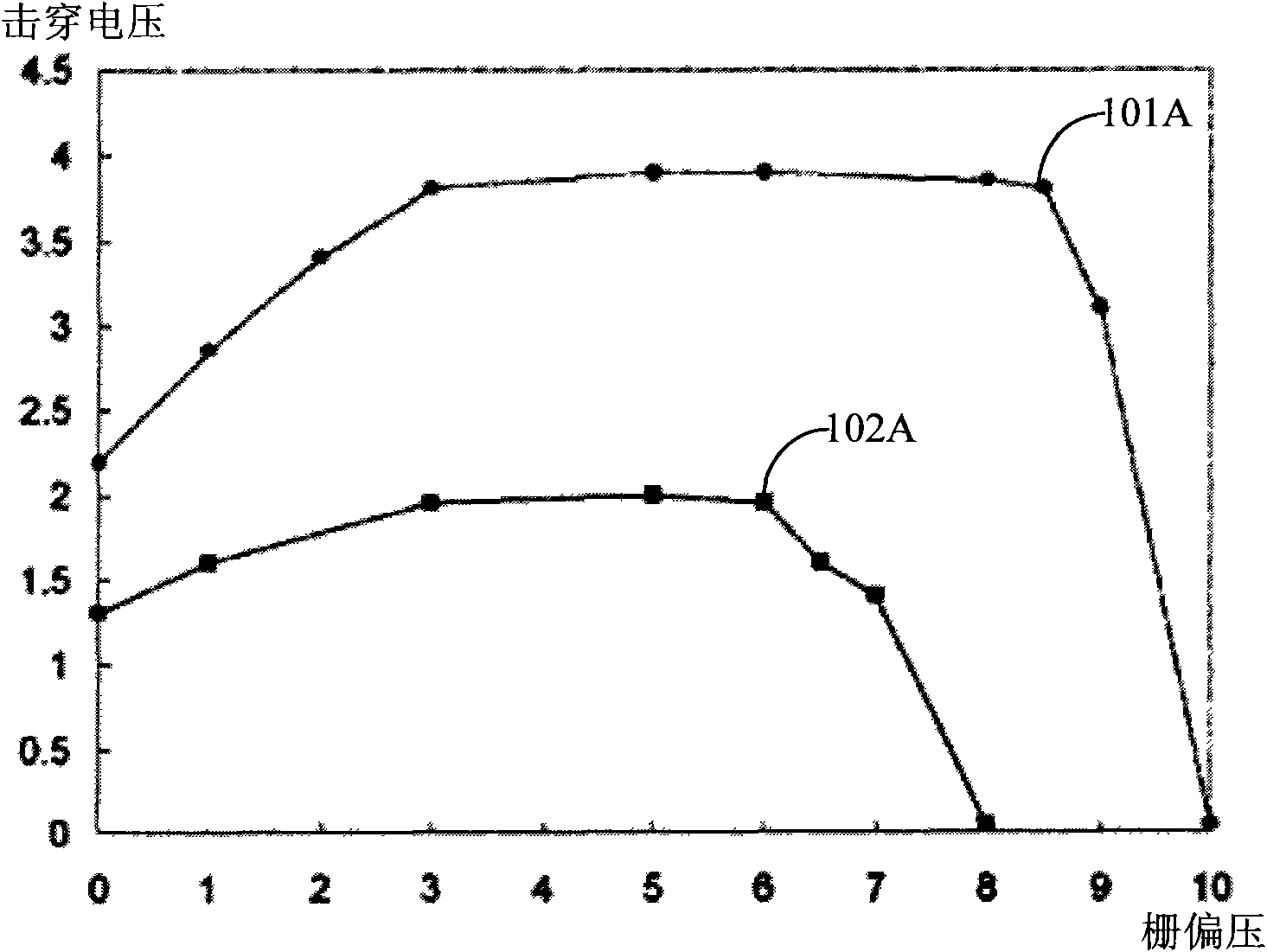
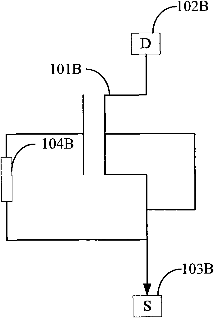
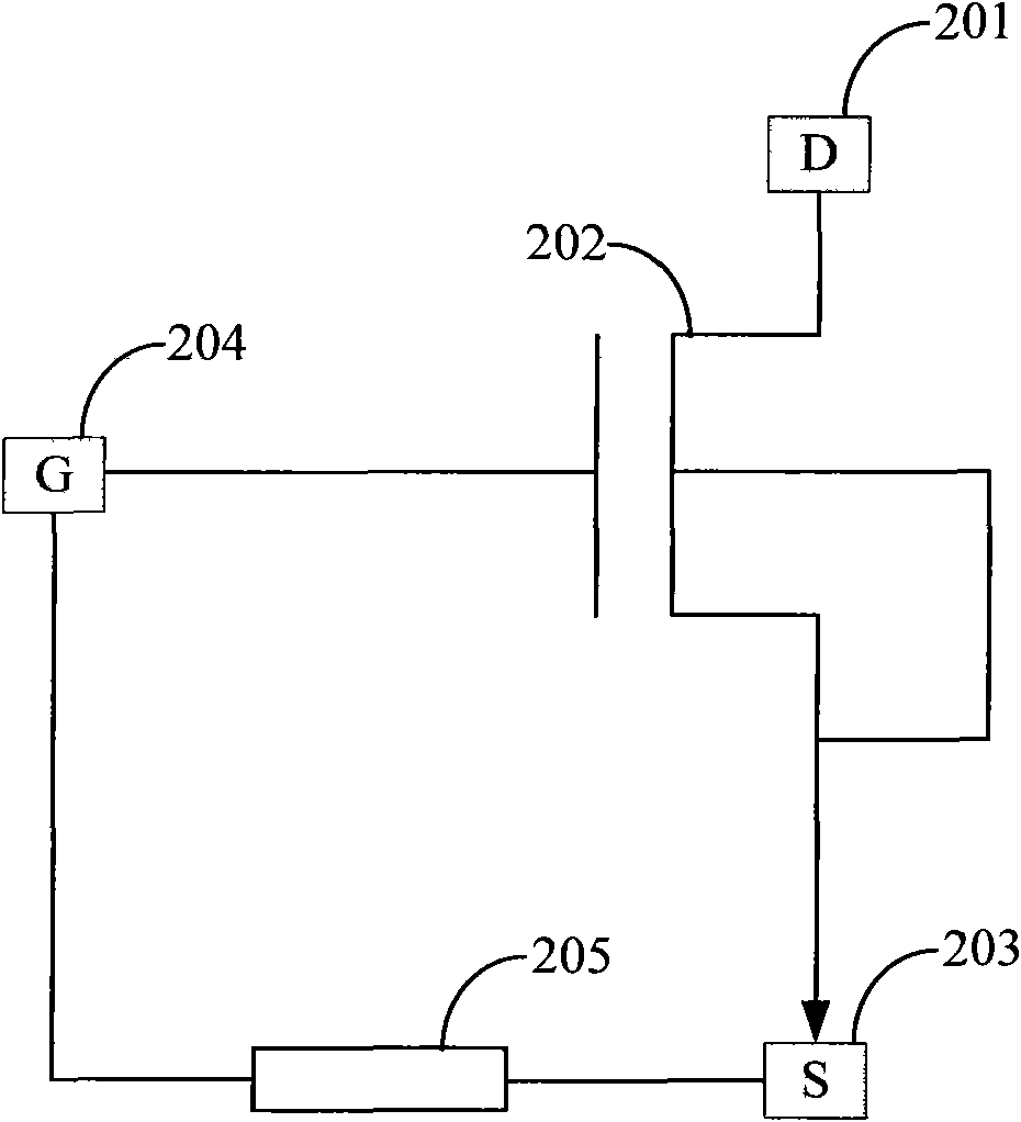
[0033] In order to thoroughly understand the present invention, detailed structures and systems will be proposed in the following descriptions, so as to illustrate how the present invention solves the electrostatic discharge test structure and system of the gate drive MOSFET. The space occupied in the layout design is large, the layout space is wasted, and the layout The problem of low design efficiency. Obviously, the practice of the invention is not limited to specific details familiar to those skilled in the semiconductor arts. Preferred embodiments of the p...


PUM


Abstract

The invention discloses an electrostatic discharge test structure of a gate-driven MOSFET (metal oxide semiconductor field effect transistor). The structure comprises an MOSFET and an adjustable resistor, wherein the gate of the MOSFET is connected with a gate bonding pad; the source of the MOSFET is connected with a source bonding pad; the adjustable resistor is connected between the gate bonding pad and the source bonding pad; and the resistance value of the adjustable resistor connected to the electrostatic discharge test structure of the gate-driven MOSFET is adjusted according to the requirement on gate offset. The invention also discloses an electrostatic discharge test system of the gate-driven MOSFET. According to the structure and system disclosed by the invention, the space occupied by the electrostatic discharge test structure of the gate-driven MOSFET and the system in the layout design can be effectively reduced, and the layout design efficiency for the electrostatic discharge test structure of the gate-driven MOSFET and the system is improved.

Description

technical field [0001] The present invention relates to the field of semiconductor technology, in particular to a gate-driven metal oxide semiconductor field effect transistor (MetatOxide Semiconductor Field Effect Transistor, hereinafter referred to as: MOSFET) electrostatic discharge (Electrostatic Discharge) test structure and system. Background technique [0002] Complementary Metal-Oxide-Semiconductor (hereinafter referred to as CMOS) technology has entered the sub-micron era, but the subsequent complexity of advanced process development has brought a lot to improve the robustness of ESD networks. difficulty. In order to solve this problem in the prior art, the robustness of the electrostatic discharge network is usually improved by adopting gate-driven technology, but the gate-driven technology needs to generate gate bias, so it needs to be solved in the layout design and development process. The problem of how to effectively generate the gate bias effect due to the g...

Claims


Application Information

Patent Timeline
Patent Type & Authority Applications(China)
IPC IPC(8): H01L25/00H01L23/60H01L23/544
CPCH01L2924/0002
Inventor 朱志炜
Owner SEMICON MFG INT (SHANGHAI) CORP
Why Eureka
Try Eureka