
Manufacture method of EEPROM (Electronically Erasable Programmable Read-Only Memory) device

A manufacturing method and device technology, applied in semiconductor/solid-state device manufacturing, electric solid-state devices, semiconductor devices, etc., can solve problems such as device failure and difficulty in adjusting the threshold voltage of low-voltage devices, so as to simplify the process steps and enhance the adjustable threshold voltage sexual effect

Active Publication Date: 2011-07-27
SHANGHAI HUAHONG GRACE SEMICON MFG CORP
View PDF2 Cites 0 Cited by
  • Summary
  • Abstract
  • Description
  • Claims
  • Application Information

AI Technical Summary

Problems solved by technology

In this way, the channel injection of low-voltage devices will be depleted by the influence of high-voltage gate oxide growth, making it difficult to adjust the threshold voltage of low-voltage devices, and eventually make the devices fail

Method used


Image

  • Manufacture method of EEPROM (Electronically Erasable Programmable Read-Only Memory) device
  • Manufacture method of EEPROM (Electronically Erasable Programmable Read-Only Memory) device
  • Manufacture method of EEPROM (Electronically Erasable Programmable Read-Only Memory) device

Examples


Embodiment Construction

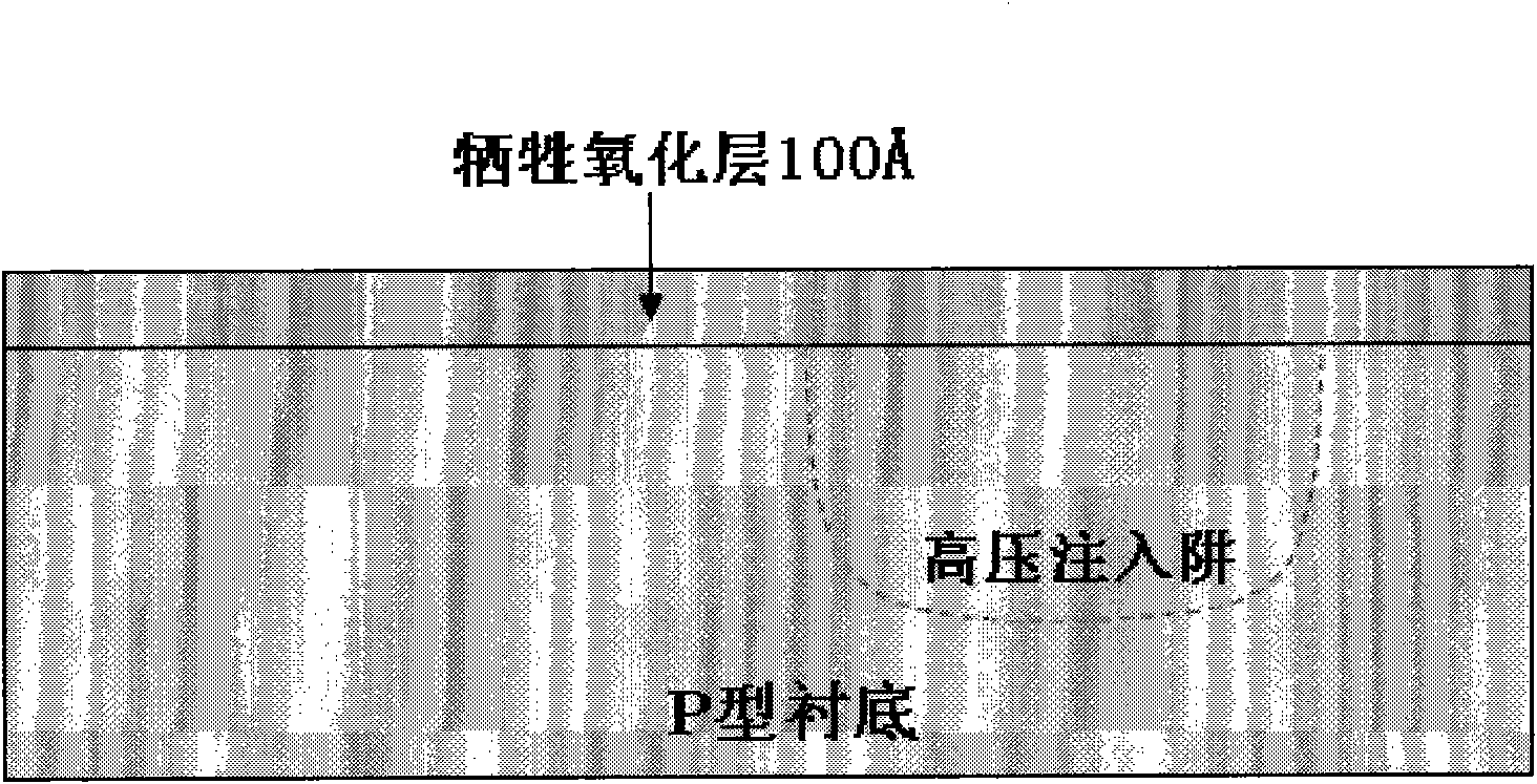
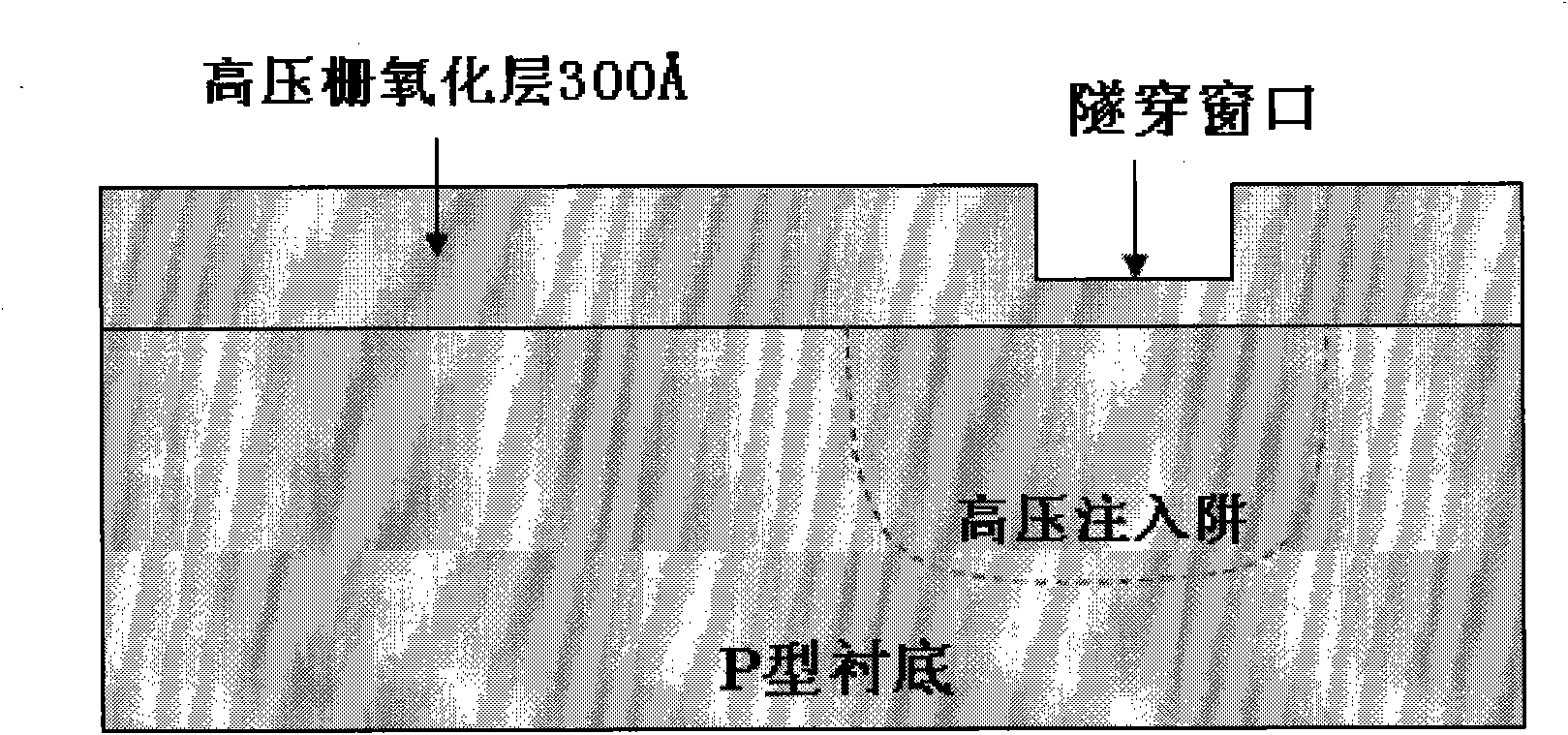
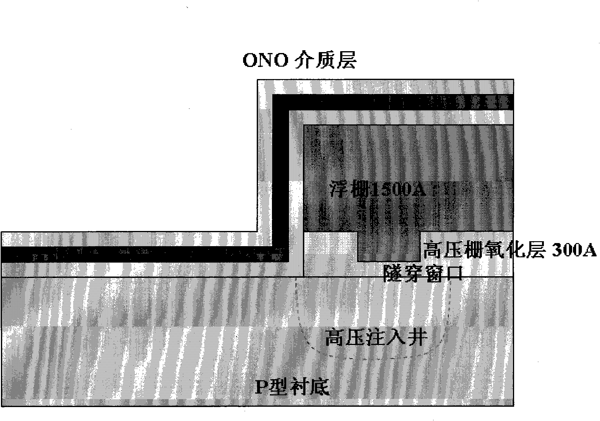
[0017] The invention provides a method for making an EEPROM device, such as Figure 1 to Figure 5 As shown, which in turn includes the following steps:

[0018] First, grow a layer of sacrificial oxide layer for high-pressure well injection to form high-pressure well injection;

[0019] Then, removing the sacrificial oxide layer, growing a high voltage gate oxide layer, and forming a tunneling window;

[0020] Afterwards, the floating gate is deposited, the floating gate is etched in the logic area, and the ONO dielectric layer is deposited, and the silicon oxide layer and the middle silicon nitride layer of the ONO dielectric layer are etched away in the logic area, and the remaining The underlying silicon oxide layer;

[0021] Finally, the silicon oxide layer at the bottom of the ONO dielectric layer that has not been etched away in the logic area is used as a sacrificial oxide layer for low-pressure well injection to form low-pressure well injection and manufacture low-vo...


PUM


Abstract

The invention discloses a manufacture method of an EEPROM (Electronically Erasable Programmable Read-Only Memory) device. The method comprises the following steps of: firstly, growing a sacrificial oxidation layer injected by a high-pressure well and forming high-pressure well injection; then, removing the sacrificial oxidation layer, growing a high-pressure grid oxidation layer and forming a tunnelling window; then, depositing a floating grid, etching off the floating grid in a logic area, depositing an ONO (Oxide-Nitride-Oxide) (Silicon Oxide / Silicon Nitride / Silicon Oxide) dielectric layer,etching off the upper layer oxidation layer and the nitrification layer of the ONO in the logic area, using the remained bottom layer oxidation layer as a retaining layer injected by a low-pressure well to form low-pressure well injection, manufacturing a low-pressure device and etching out the ONO in the logic area; and finally growing a 5-V grid oxidation layer. Through the method, the invention prevents the trench injection of a low-pressure device from being exhausted due to the influence of the oxygen growth of the high-pressure grid so as to enhance the adjustability of the threshold voltage of the low-pressure device and simplify the process steps by directly adopting the oxidation layer of the ONO dielectric layer as the sacrificial oxidation layer of low-pressure well injection.

Description

technical field [0001] The invention relates to a manufacturing method of a semiconductor memory, in particular to a manufacturing method of an EEPROM device. Background technique [0002] In the embedded EEPROM process, a variety of devices are required to achieve various functions: in the 0.18um process, 1.8V is used as a logic device, 5V is used as an input and output port device, and 18V is used as a high-voltage device to realize EEPROM operation. Integrating devices of different voltages and EEPROM memory devices is a major challenge for embedded memory technology. [0003] Traditional embedded EEPROM technology, high and low pressure well injection uses the same sacrificial oxide layer. The sacrificial oxide layer is removed after well injection, and then the high-voltage gate oxide is grown separately to form the tunneling window, floating gate and ONO (silicon oxide / silicon nitride / silicon oxide) dielectric layer, and finally the gate oxide layer of the logic low-v...

Claims


Application Information

Patent Timeline
Patent Type & Authority Applications(China)
IPC IPC(8): H01L27/115H01L29/423H01L29/788H01L21/8247H01L21/28H10B69/00
Inventor 陈昊瑜
Owner SHANGHAI HUAHONG GRACE SEMICON MFG CORP
Learn More