Manufacturing method of semiconductor device

A manufacturing method and semiconductor technology, applied in the fields of semiconductor/solid-state device manufacturing, semiconductor devices, electrical components, etc., can solve the problems of difficult overlapping capacitance, difficulty in patterning gates, etc., and achieve the effect of reducing overlapping capacitance and small device size

Active Publication Date: 2011-08-03
INST OF MICROELECTRONICS CHINESE ACAD OF SCI
View PDF0 Cites 7 Cited by
  • Summary
  • Abstract
  • Description
  • Claims
  • Application Information

AI Technical Summary

Problems solved by technology

For the gate replacement process, a typical process includes forming a dummy gate, followed by forming source / drain extensions, sidewalls, and source / drain regions, then removing the dummy gate of the device to form an opening, and then forming a replacement gate stack in the opening, The advantage of this process is that the replacement gate stack is formed after the generation of the source and drain. In this process, the gate dielectric layer and gate electrode in the replacement gate stack do not need to withstand a high annealing temperature, avoiding a high thermal budget. The possible work function transfer of the device is caused, but this process is difficult to accurately control the overlapping capacitance of the sidewall and the gate electrode and the source / drain region and the source / drain extension region, and with the continuous reduction of the gate size, the patterning The gate will become increasingly difficult

Method used


Image

  • Manufacturing method of semiconductor device
  • Manufacturing method of semiconductor device
  • Manufacturing method of semiconductor device

Examples


no. 1 example

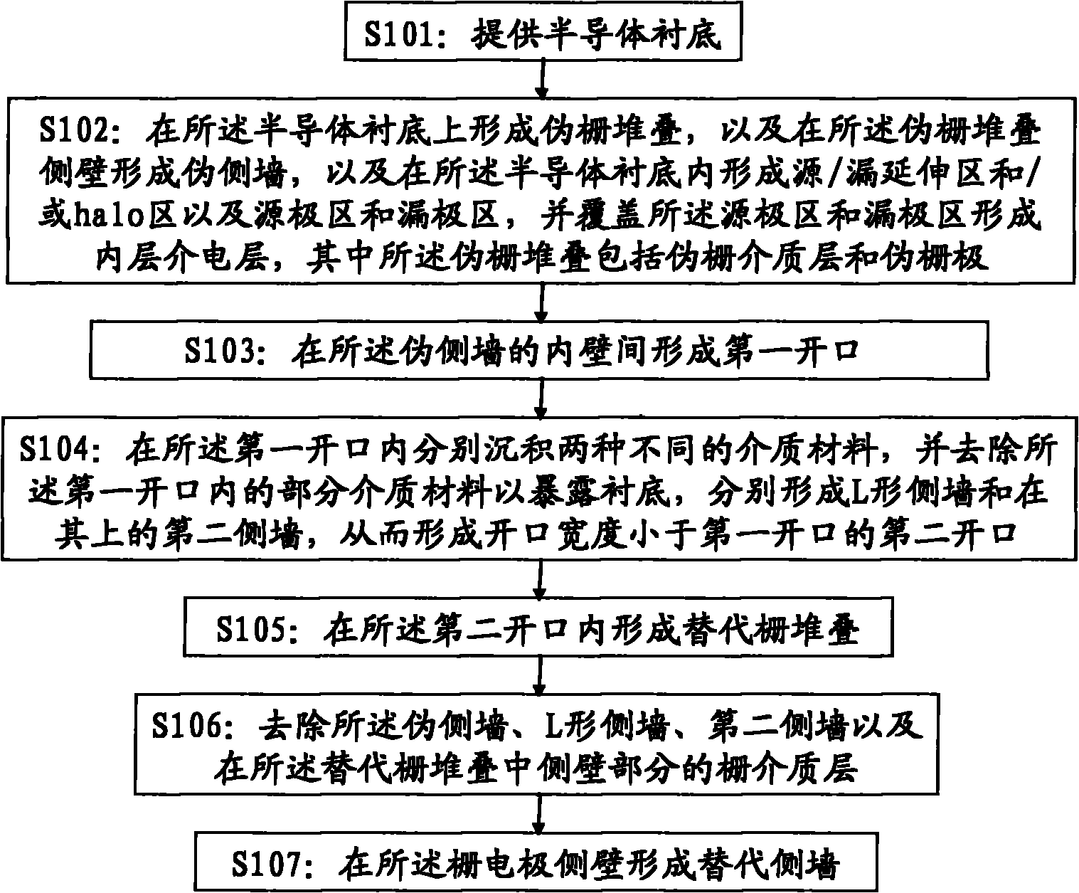
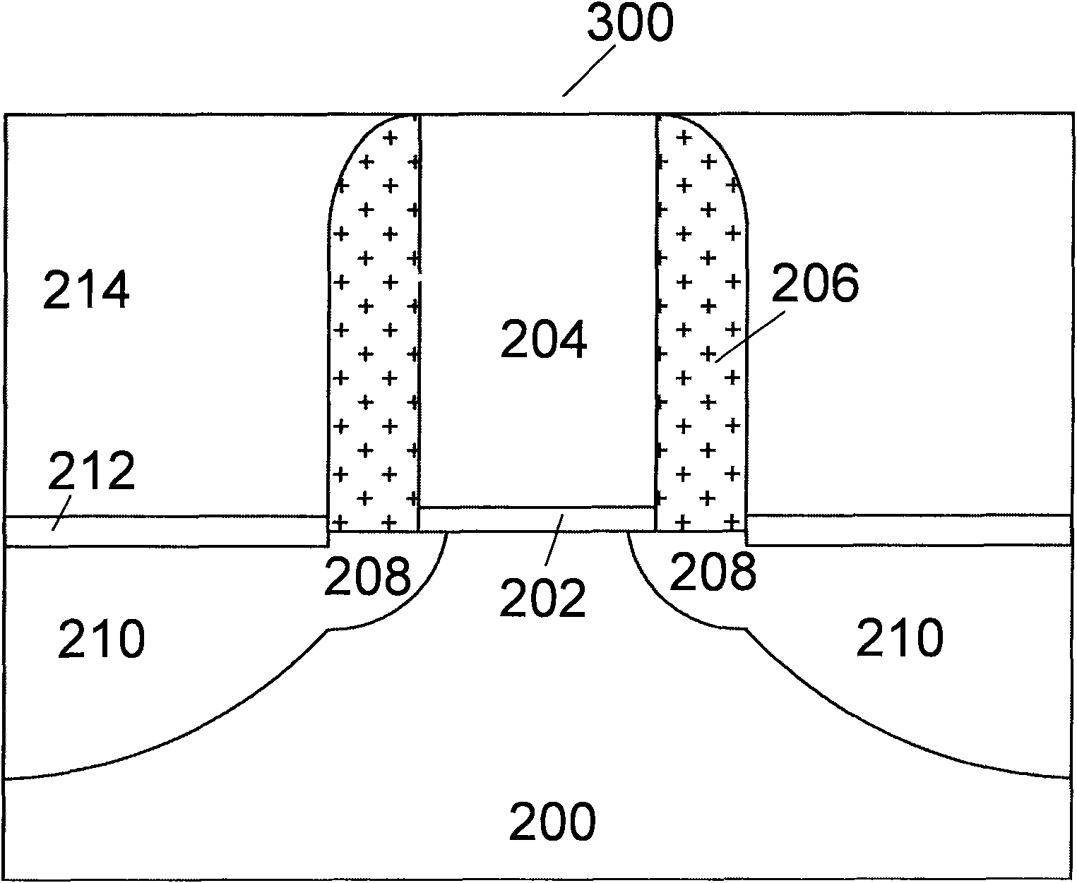
[0013] According to the first embodiment of the present invention, refer to figure 1 , figure 1 A flowchart showing a method of manufacturing a semiconductor device according to an embodiment of the present invention. In step S101, a semiconductor substrate is provided, referring to figure 2 . In this embodiment, the substrate 200 includes a silicon substrate (such as a wafer) in a crystal structure, and may also include other basic semiconductors or compound semiconductors, such as Ge, GeSi, GaAs, InP, SiC, or diamond. The substrate 200 may include various doping configurations according to design requirements known in the art (eg, p-type substrate or n-type substrate). Furthermore, the substrate 200 may optionally include epitaxial layers, may be altered by stress to enhance performance, and may include a silicon-on-insulator (SOI) structure.

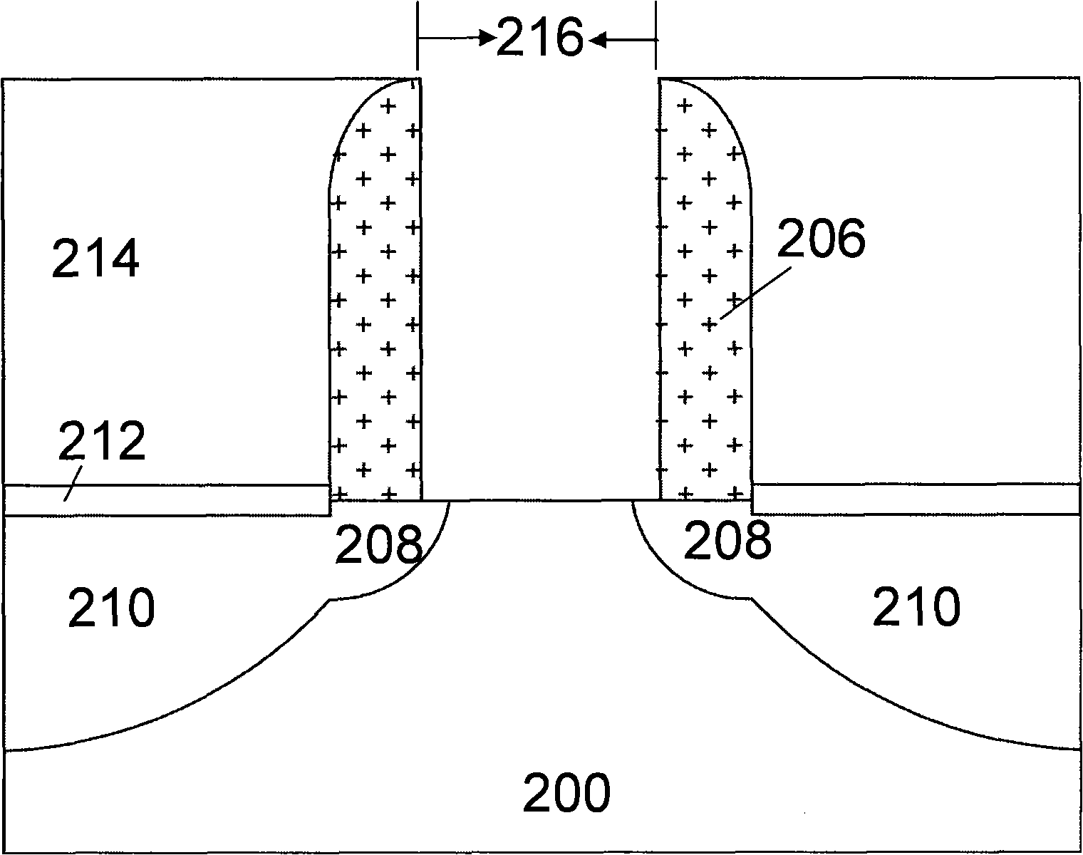
[0014] In step S102, a dummy gate stack 300 is formed on the semiconductor substrate 200, a dummy spacer 206 is formed on the s...

no. 2 example

[0027] Only the aspects of the second embodiment that differs from the first embodiment will be described below. Parts not described should be considered to be performed using the same steps, methods or processes as those in the first embodiment, so details will not be repeated here.

[0028] refer to Figure 9 , Figure 9 A flow chart showing a method for manufacturing a semiconductor device according to a second embodiment of the present invention, steps S201 to S204 according to the second embodiment of the present invention are the same as steps S101 to S104 in the first embodiment, It is considered that the same steps, methods or processes are used as those in the first embodiment, and details are not repeated here.

[0029] In step S205, the second side wall 220 is removed. The second side wall 220 can be removed by using the L-shaped side wall 218 as a stop layer by means of RIE, thereby forming the second opening 222 whose opening width is smaller than that of the f...


PUM


Abstract

The invention discloses a manufacturing method of a semiconductor device. The method comprises the following steps of: removing a pseudo-gate stack in the process of preparing a complementary metal-oxide-semiconductor (CMOS) transistor by using a replacement gate or gate last process; forming an L-shaped sidewall and a second sidewall on the L-shaped sidewall in a first opening which is formed after the pseudo-gate stack is removed; redefining the size of a replacement gate to play a role in adjusting the overlapped capacitance of a replacement gate stack and a source/drain region and a source/drain extension region; and forming a replacement sidewall by a sidewall of a gate electrode in the replacement gate stack, so that the overlapped capacitance of the sidewall and the source/drain region and the source/drain extension region is further reduced, and the whole overlapped capacitance of the device is further reduced. Furthermore, a device with a smaller size is obtained by a processmethod which is easier to implement.

Description

technical field [0001] The present invention generally relates to a manufacturing method of a semiconductor device, in particular to a manufacturing method of a semiconductor device based on a gate replacement process / gate-last process with smaller device size and small overlapping capacitance. Background technique [0002] With the development of semiconductor technology, integrated circuits with higher performance and stronger functions require greater component density, and the size, size and space of each component, between components or each component itself also need to be further reduced. In 45nm and below process integration, gate-front process and gate replacement process / gate-last process are widely used. For the gate replacement process, a typical process includes forming a dummy gate, followed by forming source / drain extensions, spacers, and source / drain regions, then removing the dummy gate of the device to form an opening, and then forming a replacement gate st...

Claims


Application Information

Patent Timeline
Patent Type & Authority Applications(China)
IPC IPC(8): H01L21/336H01L21/8238H01L21/28
Inventor 钟汇才
Owner INST OF MICROELECTRONICS CHINESE ACAD OF SCI
Why Eureka
Try Eureka