Semiconductor assembly, semiconductor device and manufacturing method

A semiconductor and component technology, applied in the field of lead-free solder layer

Active Publication Date: 2011-08-10
TAIWAN SEMICON MFG CO LTD
View PDF5 Cites 11 Cited by
  • Summary
  • Abstract
  • Description
  • Claims
  • Application Information

AI Technical Summary

Problems solved by technology

However, the melting point of the lead-free solder material is higher than that of the known tin-lead eutectic solder. Therefore, when the TCB is tested, cracks and stress reliability problems will occur, especially for large-sized dies. This problem is even more serious for

Method used


Image

  • Semiconductor assembly, semiconductor device and manufacturing method
  • Semiconductor assembly, semiconductor device and manufacturing method
  • Semiconductor assembly, semiconductor device and manufacturing method

Examples


Embodiment Construction

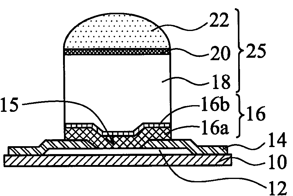
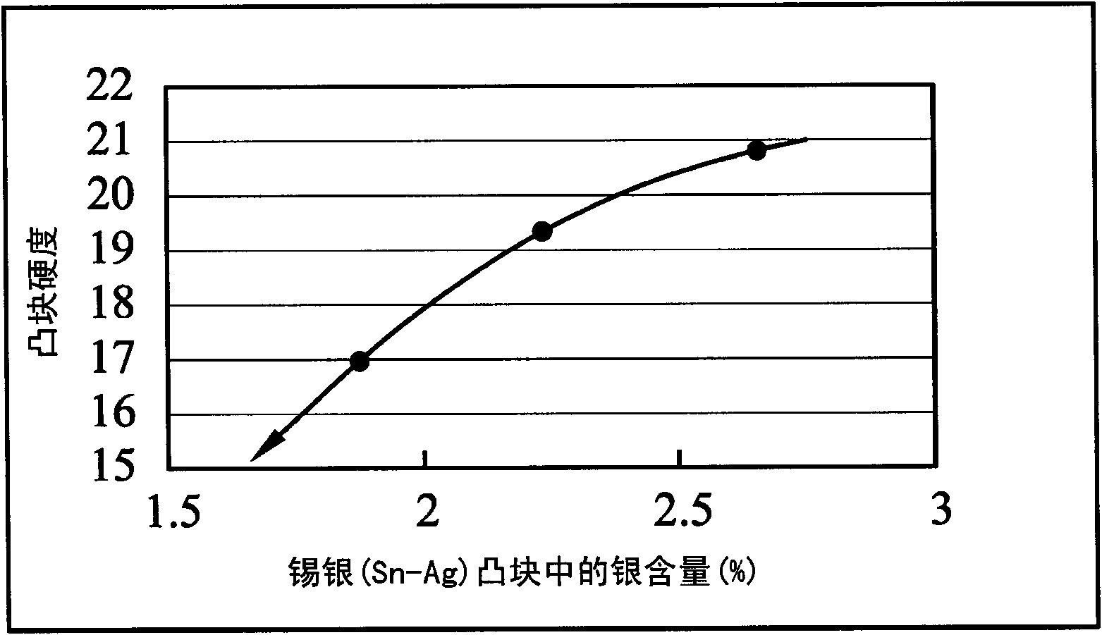
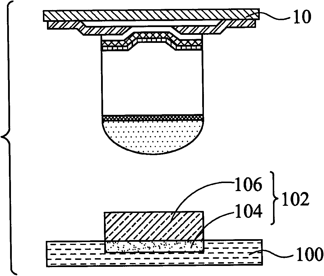
[0062] The present invention provides a lead-free solder (lead-free solder) with controlled silver content and reflow temperature, which is used for post passivation interconnects with copper post, post passivation interconnects and solder bumps , and / or semiconductor elements in which through-silicon vias (TSVs) are formed, and can be applied to flip-chip assembly (flip-chip assembly), wafer level chip scale packaging (wafer level chip scale packaging, WLCSP), three-dimensional integrated circuit stack (3D-IC stack), and / or advanced packaging technologies. In the ensuing description, specific details are set forth in order to fully understand the present invention. However, it will be understood by one of ordinary skill in the art that the present invention may be practiced without these specific details. In some embodiments, well-known structures and processes are not described in detail to avoid obscuring the present invention. "An embodiment" mentioned in the specificati...


PUM

PropertyMeasurementUnit
thicknessaaaaaaaaaa
thicknessaaaaaaaaaa
melting pointaaaaaaaaaa

Abstract

The invention provides a semiconductor assembly, a semiconductor device and a method for forming the semiconductor device. The semiconductor device includes a pad region located on the semiconductor substrate; a bump structure disposed over the pad region and electrically connected with the pad region. The bump structure includes a copper layer and a lead-free solder layer over the copper layer. The lead-free solder layer is a SnAg layer, and the Ag content in the SnAg layer is less than 1.6 weight percent. When the Ag content in the lead-free bump, the hardness of the bump will be reduced. Asofter bump could remove the crack owing to the heat stress.

Description

technical field [0001] The present invention relates to a lead-free solder layer, and in particular to a semiconductor element and a semiconductor assembly using the lead-free solder layer. Background technique [0002] Today's integrated circuits are composed of substantially millions of active elements, such as transistors and capacitors. These elements are initially isolated from each other, but are subsequently connected to form a functional circuit. Typical interconnect trenches include horizontal (latemal) interconnect structures (such as metal lines) and vertical interconnect structures (such as vias and contacts). For today's integrated circuits (ICs), the interconnect structure is increasingly important to its performance and density limits. Bond pads are formed on the uppermost layer of the interconnect structure and exposed on the surface of the corresponding chip. The chip is electrically connected to the package substrate or another die through the bond pads....

Claims


Application Information

Patent Timeline
Patent Type & Authority Applications(China)
IPC IPC(8): H01L23/485H01L21/60
CPCH01L2924/01049H01L2224/13139H01L2224/13083H01L2224/13164H01L2224/136H01L2224/81801H01L2224/13144H01L2924/01032H01L2924/01078H01L24/16H01L2224/1357H01L2224/16H01L2224/13155H01L2924/01024H01L2924/01005H01L2224/13147H01L2924/01013H01L2924/01322H01L2924/01022H01L24/13H01L2224/13109H01L24/97H01L25/50H01L2924/01012H01L21/6836H01L2224/812H01L2224/13111H01L2924/01051H01L2224/81001H01L2924/04941H01L25/0657H01L2924/0105H01L2924/01025H01L2224/97H01L2924/00013H01L2924/01327H01L2924/01047H01L2924/01046H01L24/11H01L2924/01006H01L2224/81815H01L2924/19041H01L2924/3011H01L24/94H01L2924/01079H01L2924/01073H01L2924/01074H01L2924/01038H01L2924/0103H01L2924/01082H01L2924/0104H01L2924/014H01L2224/13082H01L2924/01023H01L2924/01029H01L2225/06513H01L2924/01019H01L2224/1308H01L2221/6834H01L2924/01033H01L2924/01075H01L24/81H01L2224/023H01L2224/16237H01L2924/14H01L2924/351H01L2924/3651H01L2224/81H01L2924/00014H01L2224/13099H01L2924/00H01L2924/0001
Inventor 赖怡仁韩至刚詹前彬简智源杨怀德
Owner TAIWAN SEMICON MFG CO LTD
Why Eureka
Try Eureka