Method for manufacturing semiconductor device

A manufacturing method and semiconductor technology, applied in the direction of semiconductor devices, semiconductor/solid-state device parts, electric solid-state devices, etc., can solve the problems of high conductive resistance and low connection strength of metal layers, and achieve the effect of enhancing conductivity

Active Publication Date: 2011-08-17
NANTONG FUJITSU MICROELECTRONICS
View PDF3 Cites 8 Cited by
  • Summary
  • Abstract
  • Description
  • Claims
  • Application Information

AI Technical Summary

Problems solved by technology

The semiconductor package obtained in this way has the defects of low connection strength between the metal solder ball and the metal layer under the ball and high conductive resistance

Method used


Image

  • Method for manufacturing semiconductor device
  • Method for manufacturing semiconductor device
  • Method for manufacturing semiconductor device

Examples


Embodiment Construction

[0015] Embodiments of the present invention will be described below with reference to the drawings. Elements and features described in one drawing or one embodiment of the present invention may be combined with elements and features shown in one or more other drawings or embodiments. It should be noted that representation and description of components and processes that are not related to the present invention and known to those of ordinary skill in the art are omitted from the drawings and descriptions for the purpose of clarity.

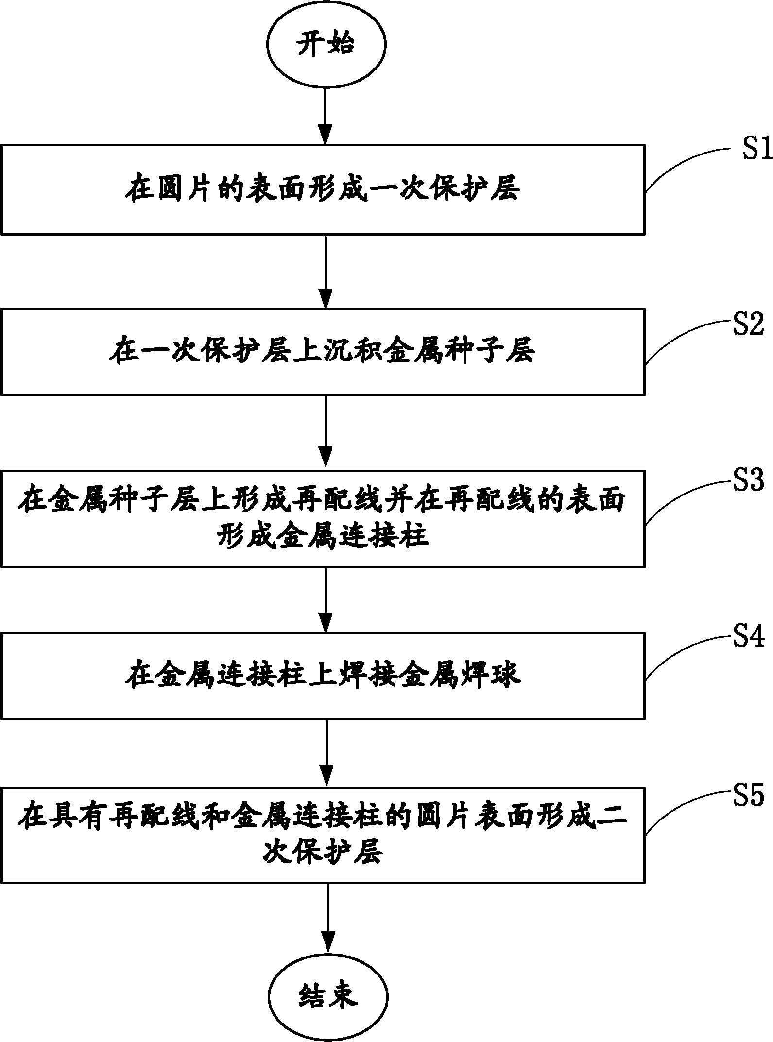
[0016] Please refer to figure 1 , one embodiment of the manufacturing method of the semiconductor device of the present invention includes the following steps.

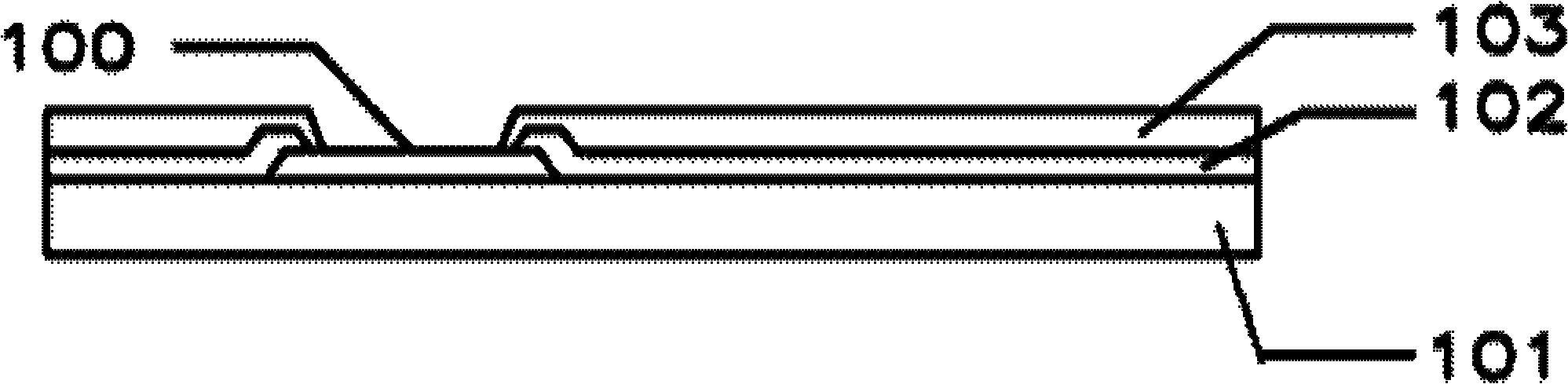
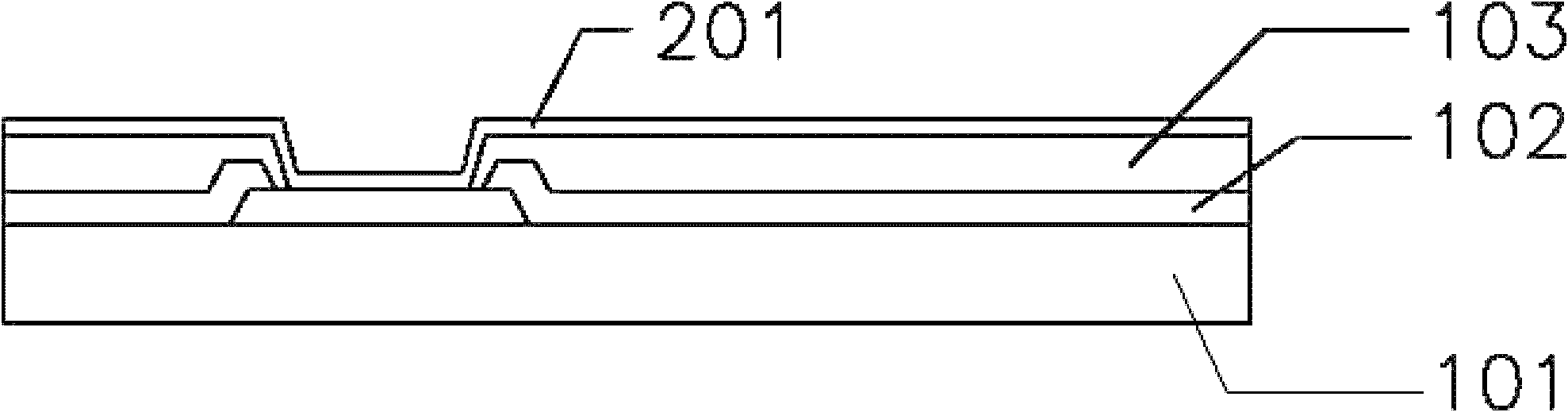
[0017] Step S1: forming a primary protective layer on the surface of the wafer. Optionally, this step includes: coating a protective material on the surface of the passivation layer 102 of the silicon wafer 101 , and performing photolithography on the coated protective material with a pr...


PUM


Abstract

The invention relates to a method for manufacturing semiconductor device, comprising the steps of: forming a primary protection layer on a disc surface; depositing a metal seed layer on the primary protection layer; forming a re-distributed wire on the metal seed layer and forming a metal connecting column on the surface of the re-distributed wire; welding a metal welded ball on the metal connecting column; and forming a secondary protection layer on the disc surface with the metal connecting column and the re-distributed wire, wherein the metal welded ball is partly exposed out of the secondary protection layer. The method related by the invention strengthens the connecting strength of the metal welded ball and the metal layer under the ball, and reduces the conductive resistance of the metal welded ball and the metal layer under the ball.

Description

technical field [0001] The present application relates to a method for manufacturing an electronic device, in particular to a method for manufacturing a semiconductor device. Background technique [0002] In recent years, the development of semiconductor packaging technology has promoted the further miniaturization of electronic products. In the past, chip packaging was achieved by pre-cutting the chip and connecting the terminals around the chip to the pins of the package carrier through metal wires in a bonding manner. With the shrinking of the chip size, the pitch of the wiring terminals is shrinking and the number is increasing, which restricts the technology of wire bonding. Wafer-level packaging (WLP) technology has improved this technical bottleneck. The WLP technology takes wafers as the processing object, on which multiple chips are packaged and tested at the same time, and finally cut into individual devices. It greatly reduces the size of the package and greatl...

Claims


Application Information

Patent Timeline
Patent Type & Authority Applications(China)
IPC IPC(8): H01L23/485
CPCH01L2224/10
Inventor 赵亚俊高国华
Owner NANTONG FUJITSU MICROELECTRONICS
Why Eureka
Try Eureka