Multilayer on-chip integrated spiral inductor with vertical structure

An integrated spiral and vertical structure technology, applied in the direction of inductors, fixed inductors, fixed signal inductors, etc., can solve the problems of obvious substrate loss and occupying a large chip area, so as to save chip area, reduce area, reduce The effect of induced current

Inactive Publication Date: 2011-08-17
HANGZHOU DIANZI UNIV
View PDF1 Cites 5 Cited by
  • Summary
  • Abstract
  • Description
  • Claims
  • Application Information

AI Technical Summary

Problems solved by technology

People's research is also mainly focused on this type of inductor. The outstanding problem of this type of inductor is that it occupies a large chip area and the substrate loss is obvious. How to effectively reduce the substrate loss and improve the quality factor is a research hotspot.

Method used


Image

  • Multilayer on-chip integrated spiral inductor with vertical structure
  • Multilayer on-chip integrated spiral inductor with vertical structure
  • Multilayer on-chip integrated spiral inductor with vertical structure

Examples


Embodiment 1

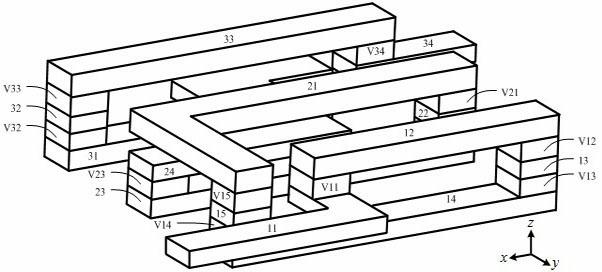
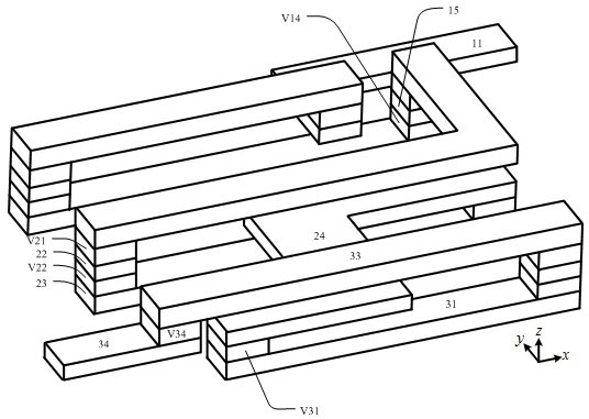
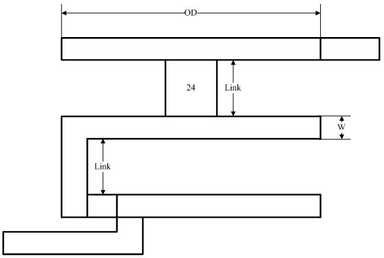
[0022] Figure 4 It is a simulation diagram of the inductance L-frequency relationship of an embodiment of the present invention. In general, the value range of the inductor line width is 4 um~14 um. In order to obtain ideal properties of the inductor, such as image 3 As shown, in this embodiment, the line width of the outer diameter of the inductor is W=8 um, OD=140 um, the length of each through hole along the x direction is also 8 um, and the distance between the inductor coils of each layer perpendicular to the horizontal plane Link=3 um, the dot curve indicates the inductance value of port 1, the triangle curve indicates the inductance value of port 2, and the low frequency inductance value can reach about 1 nH. The area required for a planar spiral inductor to achieve this inductance using the same process is about 12600 um 2 , and the area used by the inductor of the present invention is about 3380 um 2 . At the same time, the self-resonant frequency of the structu...


PUM


Abstract

The invention discloses a multilayer on-chip integrated spiral inductor with a vertical structure. In the invention, by making the inductor into a structure vertical to a horizontal plane, not only the area of the inductor covering a substrate is reduced, but also the vortexes of a common inductor, which are coupled and inducted by the magnetism of a time-varying magnetic field in the substrate, can be weakened through a laminated structure, and therefore the induction currents generated in the substrate and on the surface area of the substrate are reduced, and consequently, the effects of reducing the energy loss of the substrate and enhancing the quality factors of the inductor can be achieved.

Description

technical field [0001] The invention relates to a spiral inductor, in particular to an on-chip integrated spiral inductor. Background technique [0002] For RF IC modules, such as Low Noise Amplifiers (LNAs), Voltage Controlled Oscillators (VCOs) and matching networks, inductors are essential components. Completing the receiving circuit and matching network of the wireless clock distribution system requires an integrated inductor with a high quality factor, which makes the design of the inductor made of silicon technology particularly important. However, in the standard silicon process, the Q value (quality factor) is limited due to the resistive loss of the metal line and the loss caused by the capacitive coupling of the substrate. Recently, some non-standard processes can break through these limitations and improve the Q value, but it is expensive and difficult to complete. [0003] The traditional silicon integrated inductor is mainly planar spiral, which uses two (or m...

Claims


Application Information

Patent Timeline
Patent Type & Authority Applications(China)
IPC IPC(8): H01L27/01H01F17/00
Inventor 刘军孙玲玲
Owner HANGZHOU DIANZI UNIV
Why Eureka
Try Eureka