Optical control silicon carbide (SiC) photoconductive switch

A technology of photoconductive switch and photo-controlled silicon carbide, applied in circuits, electrical components, semiconductor devices, etc., can solve problems such as attenuation

Inactive Publication Date: 2011-08-17
SHANGHAI INST OF CERAMIC CHEM & TECH CHINESE ACAD OF SCI
View PDF3 Cites 10 Cited by
  • Summary
  • Abstract
  • Description
  • Claims
  • Application Information

AI Technical Summary

Problems solved by technology

For the switch of this structure, the incident direction of light is the very narrow side of the wafer, and the electrode is located in the center of the wafer. The SiC between the two electrodes is the area that is

Method used


Image

  • Optical control silicon carbide (SiC) photoconductive switch
  • Optical control silicon carbide (SiC) photoconductive switch
  • Optical control silicon carbide (SiC) photoconductive switch

Examples


Embodiment 1

[0098] A high-performance and high-power photoconductive switch prepared by using V-doped semi-insulating 6H-SiC single crystal as the wafer material.

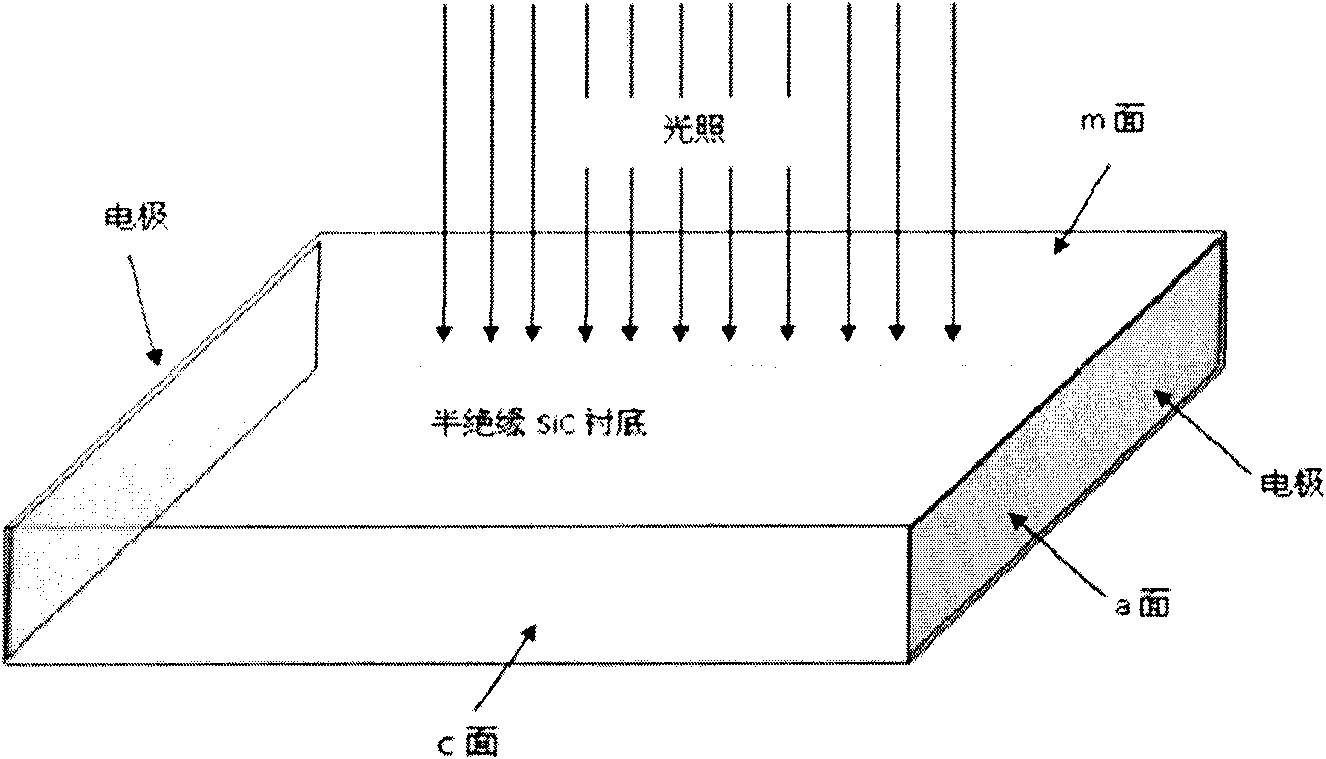
[0099] Select a V-doped semi-insulating 6H-SiC single crystal with good crystal quality ((the single crystal is grown by physical vapor transport (PVT) method, and the V doping concentration is 3.8×10 23 m -3 , the resistivity is 1.6×10 7 Ω m, the full width at half maximum of the rocking curve of the single crystal is 50 arc seconds (the parameter of crystal quality))) as the wafer material, sliced ​​into such as image 3 The cuboid structure flake shown, where l is 12mm, d is 5mm, and h is 0.4mm.

[0100] Wherein said cuboid structure is as follows:

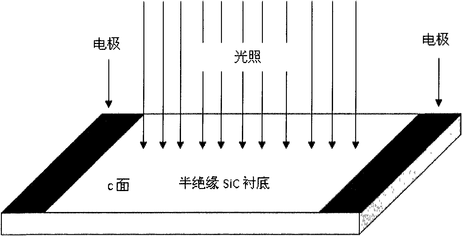
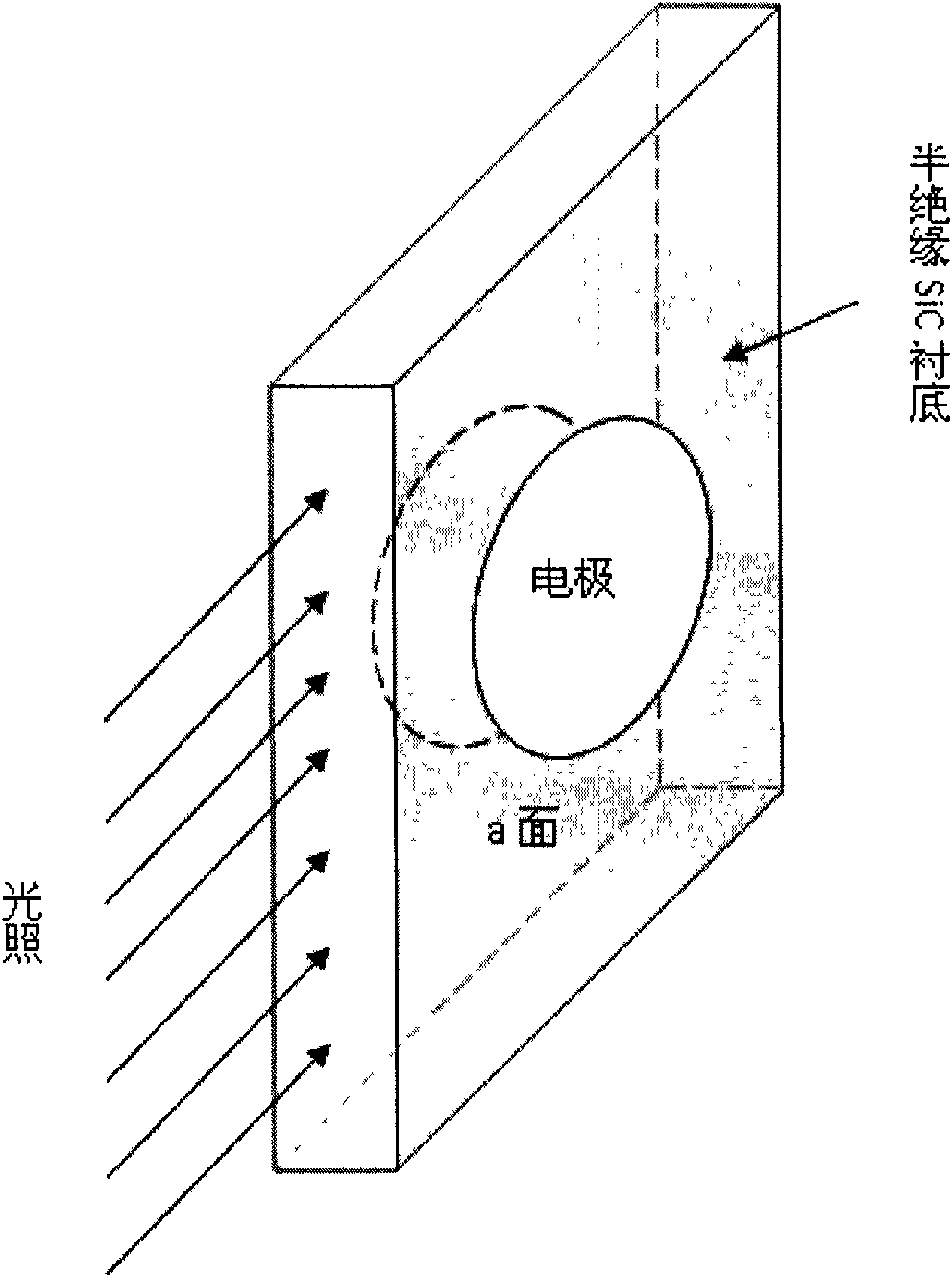
[0101] The light-facing surface is (1100), the four sides are (1120) and (0001) respectively, the backlight is (1100), and the deflection angle of each surface is less than 1 degree.

[0102] The m surface and a surface are polished to a roughness of less than 1nm. After cl...

Embodiment 2

[0105] A high-performance and high-power photoconductive switch prepared by using high-purity semi-insulating 6H-SiC single crystal as the wafer material.

[0106] Select a high-purity semi-insulating 6H-SiC single crystal with good crystal quality (the single crystal is grown by physical vapor transport (PVT) method, and the V doping concentration is less than 7.6×10 20 m -3 , the resistivity is 1.0×10 7 Ω m, the half-maximum width of the rocking curve of this single crystal is 45 arc seconds (the parameter of crystallization quality)) as the wafer material, sliced ​​into such as image 3 The flakes shown, where l is 12 mm, d is 5 mm, and h is 0.5 mm. The surface m and surface a are polished to a roughness of less than 1nm, cleaned by the standard RCA process, annealed at 1200°C for 3 hours in hydrogen with a pressure of 1 bar to eliminate the surface damage layer, and then soaked in HF acid with a concentration of 10% for 12 Rinse with pure water for 30 minutes before use...

Embodiment 3

[0109] A high-performance and high-power photoconductive switch prepared by using V-doped semi-insulating 4H-SiC single crystal as the wafer material.

[0110] Select a V-doped semi-insulating 4H-SiC single crystal with good crystal quality (the single crystal is grown by physical vapor transport (PVT) method, and the V doping concentration is 6.1×10 22 m -3 , the resistivity is 3.5×10 7 Ω m, the half-maximum width of the rocking curve of this single crystal is 40 arc seconds (the parameter of crystal quality)) as the wafer material, sliced ​​into such as image 3 The flakes shown, where l is 12 mm, d is 5 mm, and h is 0.5 mm. The surface m and surface a are polished to a roughness of less than 1nm, cleaned by the standard RCA process, annealed at 1200°C for 3 hours in hydrogen with a pressure of 1 bar to eliminate the surface damage layer, and then soaked in HF acid with a concentration of 10% for 12 Rinse with pure water for 30 minutes before use, cover the mask, put it i...


PUM

PropertyMeasurementUnit
Wavelengthaaaaaaaaaa
Pressure valueaaaaaaaaaa

Abstract

The invention relates to an optical control silicon carbide (SiC) photoconductive switch. The switch comprises the following components: a SiC photoconductive wafer and electrodes electrically connected with (1120)a surface(s) or (1120)m surfaces, wherein the SiC photoconductive wafer has the following well polished crystal planes: at least a (1100)m surface and at least two (1120)a surfaces; the (1100)m surfaces or the (1120)a surfaces are sunward surfaces optically connected with excitation light sources; when the (1100)m surfaces serve as the sunward surfaces, the electrodes are electrically connected with the (1120)a surface(s); and when the (1120)a surfaces serve as the sunward surfaces, the electrodes are electrically connected with the (1100)m surfaces.

Description

technical field [0001] The invention relates to a light-controlled silicon carbide photoconductive switch, in particular to a light-controlled high-power silicon carbide (SiC) photoconductive switch withstanding high voltage and high current, which belongs to the technical field of high-power semiconductor switch device preparation. Background technique [0002] Switches are one of the essential components in power electronic circuits, and the properties of switches are particularly important in high-power systems. The so-called high-power system must withstand large voltage and current at the same time. The most direct problem that a large voltage brings to the device is the avalanche breakdown caused by the acceleration of the carrier by the strong electric field, and the thermal breakdown is easy to occur due to the thermal effect under the high current. These two failure modes are difficult problems faced by high-power switching devices. The high-power switch currently...

Claims


Application Information

Patent Timeline
IPC IPC(8): H01L31/09H01L31/0224H01L31/18
CPCH01L31/022408H01L31/09H01L31/08
Inventor 黄维常少辉陈之战施尔畏
Owner SHANGHAI INST OF CERAMIC CHEM & TECH CHINESE ACAD OF SCI
Why Eureka
Try Eureka