Nitride LED structure and preparation method thereof

A technology of LED structure and nitride, which is applied in the direction of electrical components, circuits, semiconductor devices, etc., can solve crystal defects, reduce crystal quality and other problems, and achieve the effect of promoting phase separation, improving internal quantum efficiency and luminous intensity

Inactive Publication Date: 2011-08-17
ENRAYTEK OPTOELECTRONICS
View PDF8 Cites 32 Cited by
  • Summary
  • Abstract
  • Description
  • Claims
  • Application Information

AI Technical Summary

Problems solved by technology

[0010] However, in the above method, due to the difference in lattice constant between InGaN and GaN, a heterojunction will be formed, resulting in crystal defects and reducing the quality of the crystal.

Method used


Image

  • Nitride LED structure and preparation method thereof
  • Nitride LED structure and preparation method thereof
  • Nitride LED structure and preparation method thereof

Examples


Embodiment Construction

[0039] The structure and preparation method of the nitride LED proposed by the present invention will be further described in detail below with reference to the accompanying drawings and specific examples. Advantages and features of the present invention will be apparent from the following description and claims. It should be noted that all the drawings are in very simplified form and use imprecise ratios, which are only used for the purpose of conveniently and clearly assisting in describing the embodiments of the present invention.
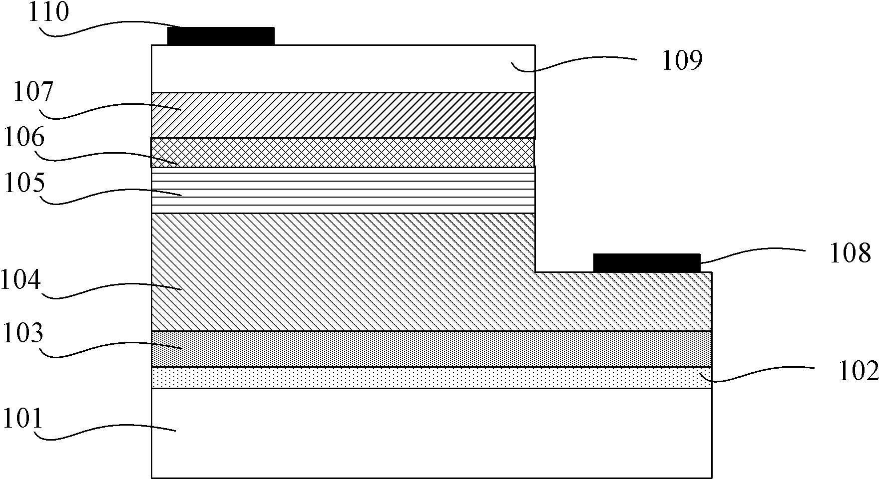
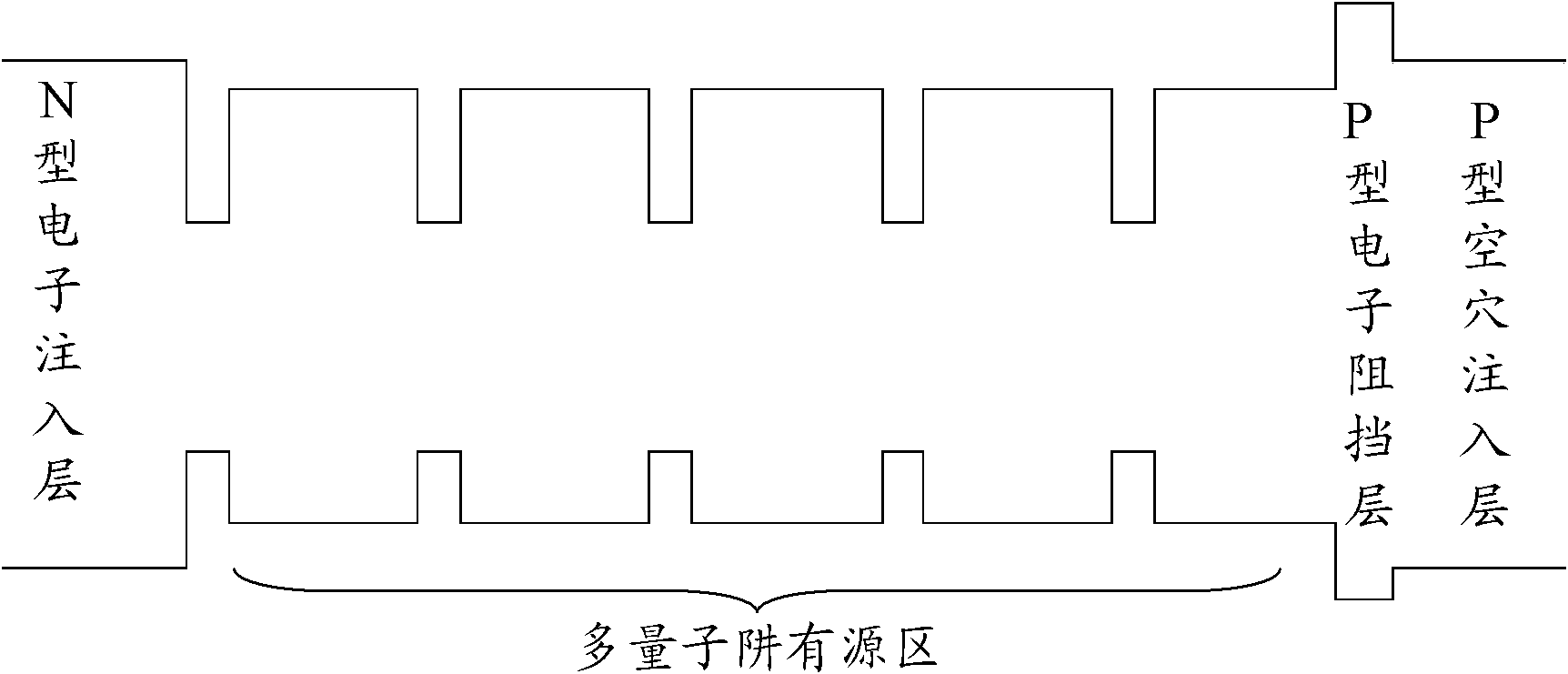
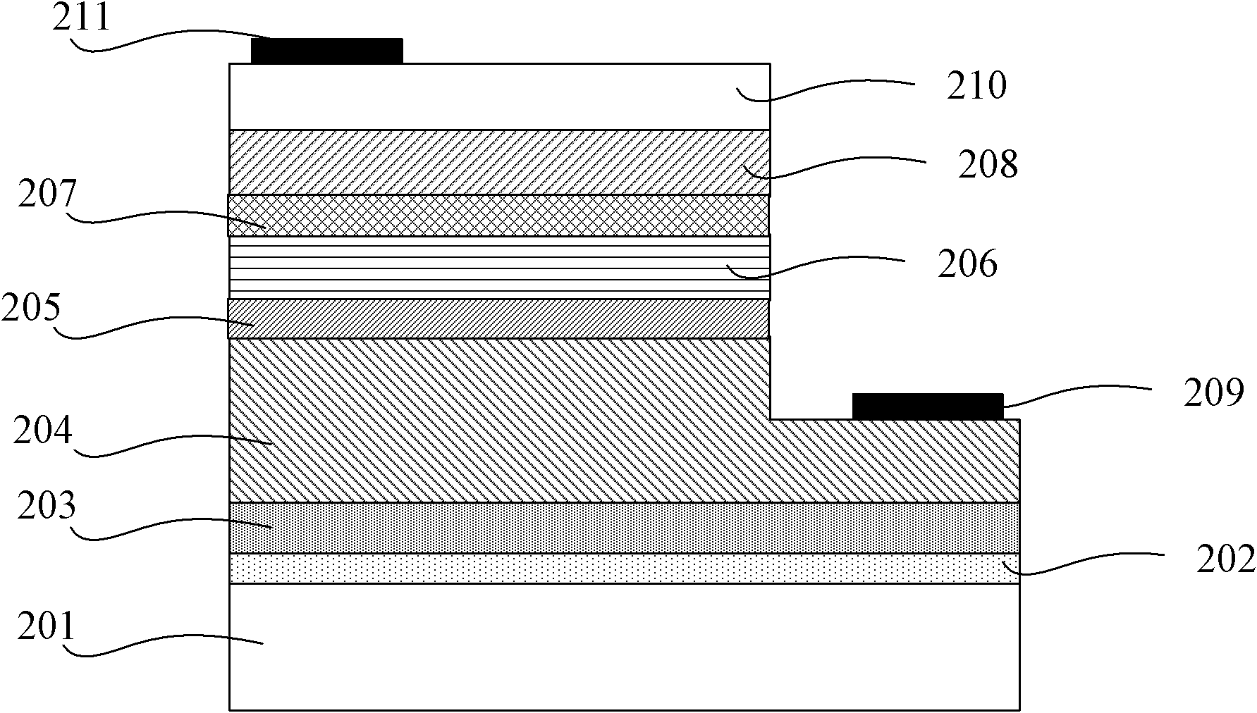
[0040] The core idea of ​​the present invention is to provide a nitride LED structure, which inserts an InGaN layer with gradually changing In content between the N-type electron injection layer and the multi-quantum well active layer, thereby releasing the multi-quantum well active layer and the N The stress between the N-type electron injection layer improves the internal quantum efficiency and luminous intensity of the device; at the same tim...


PUM


Abstract

The invention discloses a nitride light-emitting diode (LED) structure. An indium gallium nitrogen (InGaN) layer with gradually varied indium (In) content is inserted between an N-type electron injection layer and a multi-quantum well active layer so as to release a stress between the multi-quantum well active layer and the N-type electron injection layer and improve the internal quantum efficiency and the luminous intensity of a device. The invention also discloses a preparation method for the nitride LED structure. In the method, the InGaN layer with gradually varied In content is inserted between the N-type electron injection layer and the multi-quantum well active layer so as to release the stress between the multi-quantum well active layer and the N-type electron injection layer and improve the internal quantum efficiency and the luminous intensity of the device.

Description

technical field [0001] The invention relates to the technical field of LED preparation, in particular to a nitride LED structure and a preparation method thereof. Background technique [0002] A light-emitting diode (LED, Light Emitting Diode) is a semiconductor solid-state light-emitting device, which uses a semiconductor PN junction as a light-emitting material, and can directly convert electricity into light. When a forward voltage is applied to both ends of the semiconductor PN junction, the minority carriers injected into the PN junction recombine with the majority carriers, releasing energy to cause photon emission, and the colors are red, orange, yellow, green, and red. Cyan, blue, purple light. [0003] With the development of nitride-based high-brightness LED applications, a new generation of green and environmentally friendly solid-state lighting sources-nitride LEDs has become the focus of attention. Group III nitride semiconductor materials mainly composed of G...

Claims


Application Information

Patent Timeline
Patent Type & Authority Applications(China)
IPC IPC(8): H01L33/06H01L33/32H01L33/00
Inventor 于洪波
Owner ENRAYTEK OPTOELECTRONICS
Why Eureka
Try Eureka