

One time programmable (OTP) resistive random access memory (RRAM) as well as read-write circuit and programming method thereof
A technology of random access memory and read-write circuit, applied in the field of read-write circuit, can solve the problems of low safety performance and small area of OTP memory data storage, and achieve the effects of low power consumption, simple pulse signal, and small area
- Summary
- Abstract
- Description
- Claims
- Application Information
AI Technical Summary
Problems solved by technology
Method used
Image

Examples
Embodiment Construction
[0036] In order to make the object, technical solution and advantages of the present invention clearer, the present invention will be further described in detail below in conjunction with the accompanying drawings.
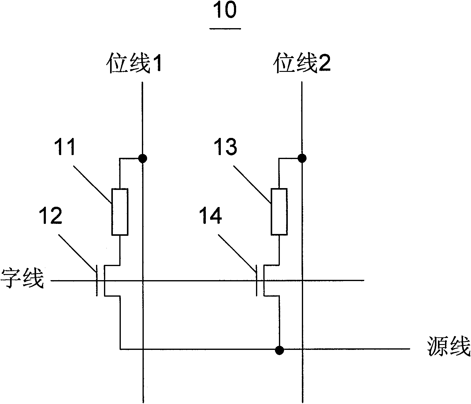
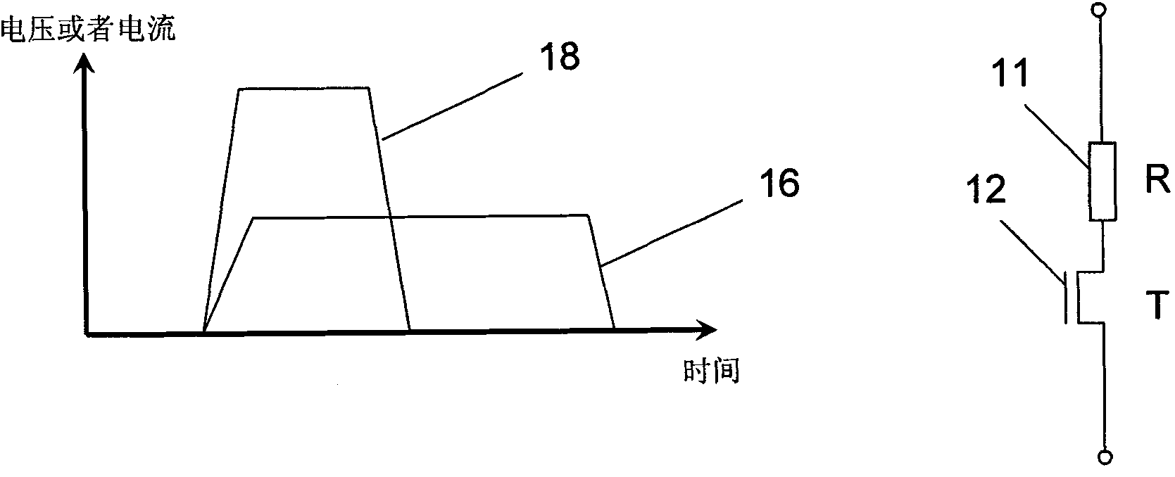
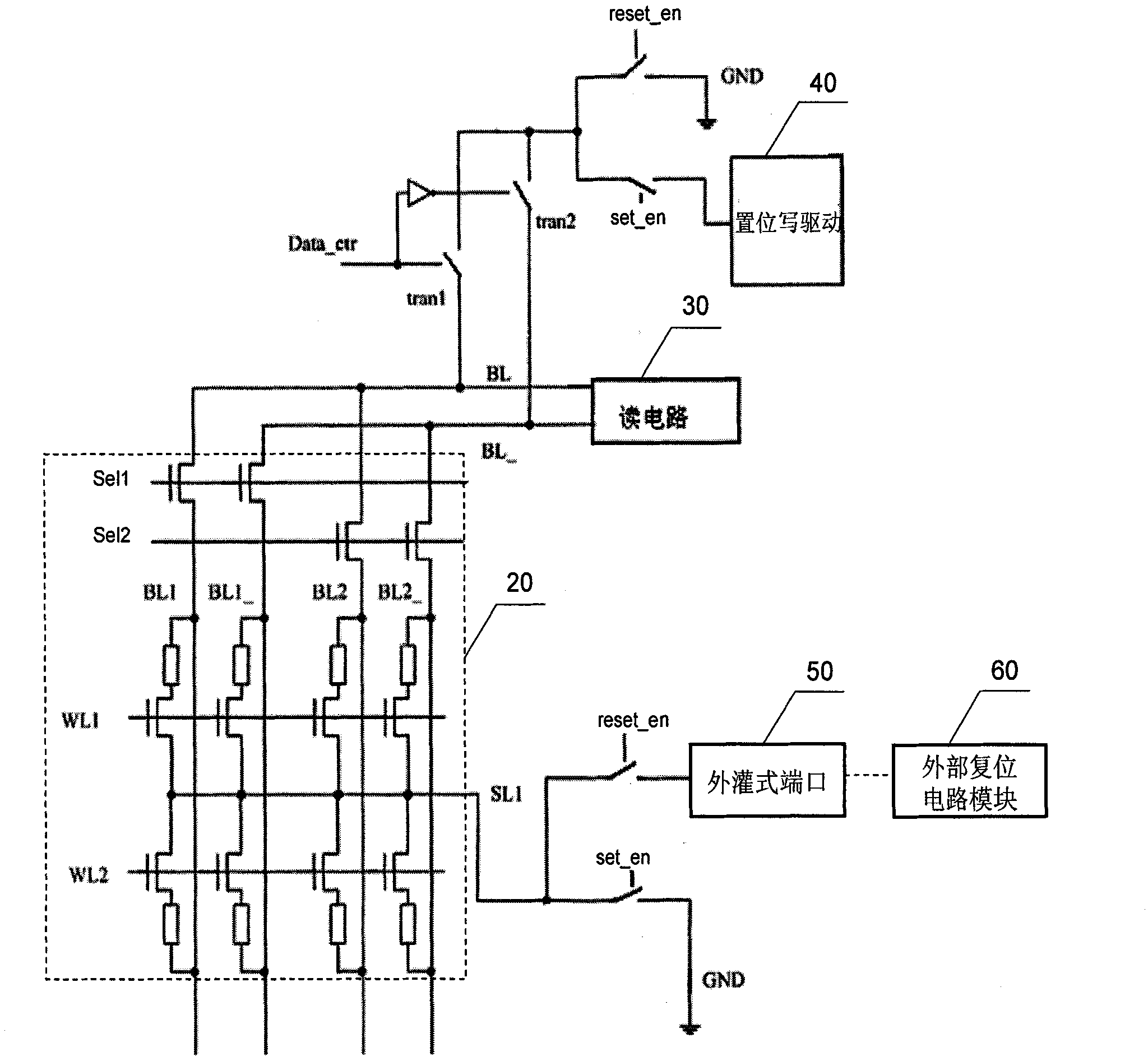
[0037] figure 1 Shown is a schematic structural diagram of the OTP resistance random access memory provided by the embodiment of the present invention. Such as figure 1As shown, the OTP resistance random access memory 10 of a memory cell is given. The OTP RRAM 10 includes a first storage resistor 11 , a first gate transistor 12 connected in series with the first storage resistor, a second storage resistor 13 , and a second gate transistor 14 connected in series with the second storage resistor. The storage resistance is defined as R (Resistance), and the gate tube is defined as T (Transistor), so the resistance RAM has a 2T2R structure. In this embodiment, one end of the first storage resistor 11 is connected in series with the first gate tube 12, and the other...
PUM
 Abstract
Description
Claims
Application Information