Protection panel provided with touch input function for electronic device display window
A technology for touch input and electronic equipment, applied in the input/output process of data processing, printed circuits, electrical components, etc., can solve the problems of poor appearance quality, easy change of interval size, and reduced connection reliability of FPC110, so as to improve the connection Reliability, improve appearance quality, improve the effect of conduction reliability
- Summary
- Abstract
- Description
- Claims
- Application Information
AI Technical Summary
Problems solved by technology
Method used
Image
Examples
Embodiment 1
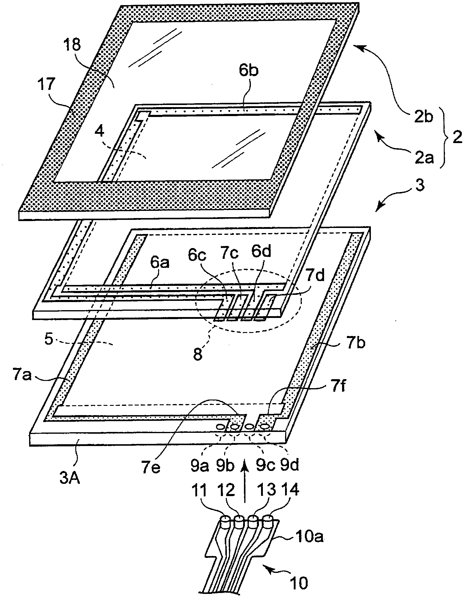
[0136] An ITO film with a thickness of 20 nm was formed by sputtering on the entire surface of one surface of a PET film with a thickness of 0.1 mm as a substrate for forming the lower transparent electrode, and the peripheral part of the ITO film was removed to form a wide rectangular shape. The lower transparent electrode 5. Furthermore, bus bars 7a, 7b and lead-out lines 7e, 7f for outputting from the bus bars to the outside are respectively formed by screen printing using silver paste, and the bus bars 7a, 7b are arranged along the bottom transparent electrode 5. Horizontally opposite sides. In addition, an acrylic resin plate with the same vertical and horizontal dimensions as the PET film and a thickness of 0.7 mm is used as the protective panel body 3A, and is bonded to the PET film using a substrate-free transparent adhesive with a thickness of 0.025 mm. After the surface opposite to the surface on which the lower transparent electrode 5 is formed, four through holes ...
Embodiment 2
[0145] The dot spacers 30 are formed on the periphery of the through-holes 9 a to 9 d on the upper surface of the lower electrode panel 3 instead of on the upper electrode sheet 2 a side, and are the same as in the first embodiment. .
Embodiment 3
[0147] Embodiment 3 is the same as Embodiment 1 except that the spacers 30 are formed on the peripheral portions of the through holes 9 a to 9 d on the upper surface of the lower electrode panel 3 . That is, in Embodiment 3, it is an example as follows: the dot spacer 30 is as Figure 8 The figure is fixed to the peripheral edge portions of the through holes 9 a to 9 d on the upper surface of the lower electrode panel 3 and the upper electrode sheet 2 a.
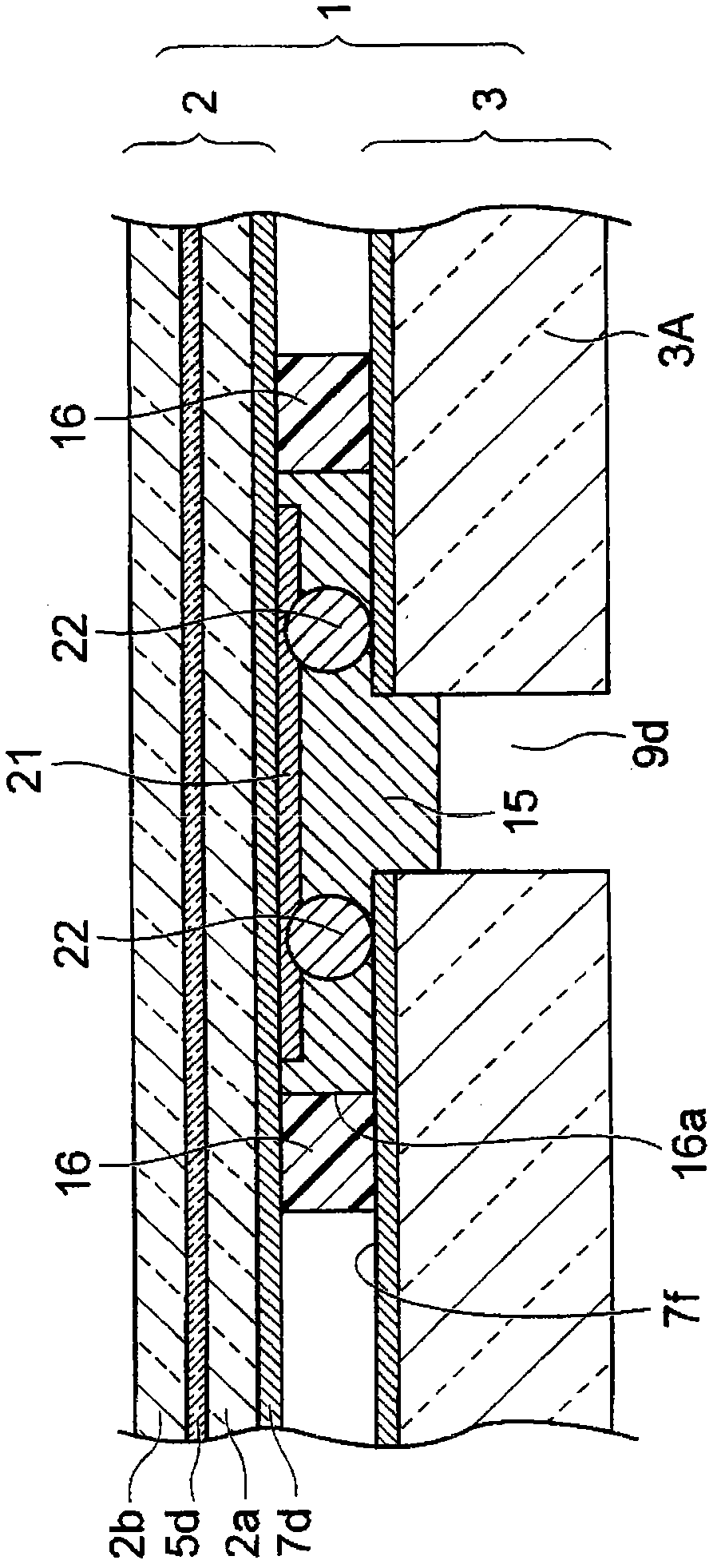
[0148] The protective panels 1 with a touch input function of the above-mentioned embodiments 1 to 3 are all separated from each other between the peripheral parts of the through holes 9 a to 9 d on the upper surface of the lower electrode panel 3 and the upper electrode sheet 2 . A plurality of dot spacers 30 are fixedly arranged at intervals, and the gaps maintained by the dot spacers 30 are filled with conductive adhesive 15 from the through holes 9a to 9d. Therefore, the connection reliability of the FPC 10 and the prote...
PUM
 Abstract
Description
Claims
Application Information


