
Silver nanometer material and application thereof

A technology of silver nanometer and silver nanoparticle, applied in nanotechnology, nanotechnology, nano-optics and other directions, can solve problems such as increased insertion loss and high pump power

Inactive Publication Date: 2011-09-14
HUAZHONG UNIV OF SCI & TECH
View PDF2 Cites 2 Cited by
  • Summary
  • Abstract
  • Description
  • Claims
  • Application Information

AI Technical Summary

Problems solved by technology

However, due to the plasmon resonance absorption of metals, the insertion loss becomes larger and higher pump power is required

Method used


Image

  • Silver nanometer material and application thereof
  • Silver nanometer material and application thereof
  • Silver nanometer material and application thereof

Examples


preparation example Construction

[0012] 1. Preparation of silver nanomaterials

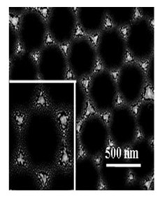
[0013] The preparation of the silver nano material of the present invention can adopt the nanosphere etching method, "natural etching technique", and nanosphere etching technology, and the nanosphere etching technique is recommended here. The following is a detailed description of the nanosphere etching technology:

[0014] (1) Preparation of nanosphere mask plate;

[0015] Required materials: polystyrene nanospheres (Duke Scientific Corp) with a diameter of 450±5nm, quartz substrate (10×10×0.2mm3), methanol, ethanol, sodium dodecylsulfate (dodecylsodiumsulfate, SDS), de ionized water. In addition, a vertical puller, a petri dish (7-9cm in diameter) and a micro-sampler (50uL) are required;

[0016] Substrate cleaning: soak the quartz substrate in piranha solution (3:1H2SO4:30%H2O2) at 80oC for 1.5 hours, wash it repeatedly with distilled water after cooling, and then ultrasonically clean it in 5:1:1H2O:NH4OH:30%H2O2 Bath for ...

example 1

[0024] Example 1 Double beam interference switch

[0025] Such as figure 2 As shown, the optical path is a typical two-beam interference structure, and the optical switching effect is realized through this simple structure. The two beams of light indicated in red are obtained by splitting the same laser beam, and the sample of the silver nanoparticle array described above is added to one of the beams. The adjustment makes the two paths of light have the same optical path, that is, they have the same phase, so that the effect of interference enhancement can be achieved. Since the power density of the signal light is weak, it is not enough to excite the nonlinear effect in the sample. At this time, a beam of laser light with a strong power density is incident on the sample (shown as the blue beam), and incident on the same area of ​​the sample as the signal light. Due to the nonlinear effect of silver nanoparticles, the signal of this channel will Light produces a nonlinear ...

example 2

[0026] Example 2 Light-controlled ultrafast switch

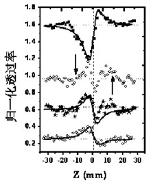
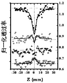
[0027] if will figure 2 The excitation light and signal light in the system are also consistent in time, that is, the phase difference between the pump light and the signal light can be fine-tuned through the optical delay line, so that the pump light reaches the sample ahead of the signal light. Such as image 3 As shown, in a short time (~1 ps) after the excitation light is applied, the signal light transmittance changes suddenly, and then after about 40 ps, ​​the signal light transmittance basically returns to the original state, indicating that the recovery time of the optical switch prepared by this sample is within On the order of picoseconds, it meets the needs of ultrafast optical switches.


PUM

PropertyMeasurementUnit
Diameteraaaaaaaaaa
Particle sizeaaaaaaaaaa

Abstract

The invention provides a silver nanometer material and application thereof. The silver nanometer material has a periodical structure formed by hexagonal silver nanometer particle arrays, and is suitable for preparing an ultra-fast optical switch with a near ultraviolet waveband of 350 to 450 nanometers. The silver nanometer material provided by the invention has a very high nonlinear refractive index in a resonance region of the silver; a switching speed of the near ultraviolet waveband ultra-fast optical switch prepared from the silver nanometer material can reach a sub-picosecond scale, and therefore the loss caused by the metal surface plasma resonance absorption is greatly reduced.

Description

technical field [0001] The invention relates to the field of nanometer materials, and specifically relates to a silver nanometer material, which is suitable for preparing an ultrafast optical switch in the 350-450 near-ultraviolet band. Background technique [0002] With the development of society and the explosive growth of data services represented by IP, new high-speed and large-capacity transmission technologies have emerged to meet the ever-increasing bandwidth requirements of the network, making the network finally fully optical (data from source nodes to destinations) The transmission process of the nodes is carried out in the optical domain) and the network direction develops. Along with the development of all-optical network, the development and application of various all-optical network equipment and devices have attracted people's attention and attention. Optical switches and optical switch arrays are precisely the core technologies in these core devices. In ter...

Claims


Application Information

Patent Timeline
IPC IPC(8): C23C14/14C23C14/28G02F1/355B82Y20/00
Inventor 陆培祥王凯王少义杨光龙华付明
Owner HUAZHONG UNIV OF SCI & TECH
Learn More