

Method for preparing diamond-silicon carbide electronic packaging material fast
An electronic packaging material, diamond technology, applied in circuits, electrical components, electric solid devices, etc., can solve the limitations of large-scale production and application of diamond-silicon carbide composite materials, limited performance of second-generation packaging materials, and single preparation methods, etc. problem, to achieve the effect of low-cost preparation, high mechanical and thermal properties, and simple preparation process
- Summary
- Abstract
- Description
- Claims
- Application Information
AI Technical Summary
Problems solved by technology
Method used
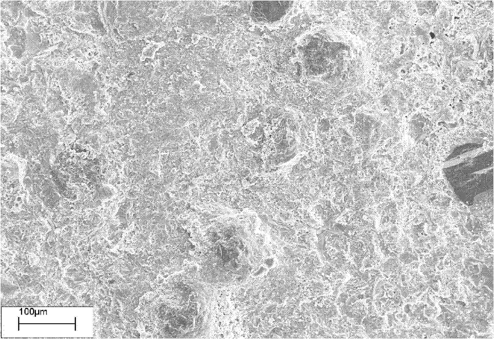
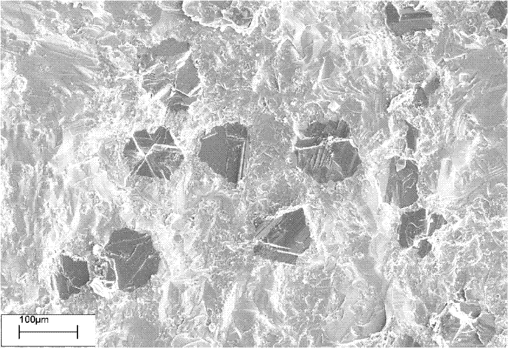
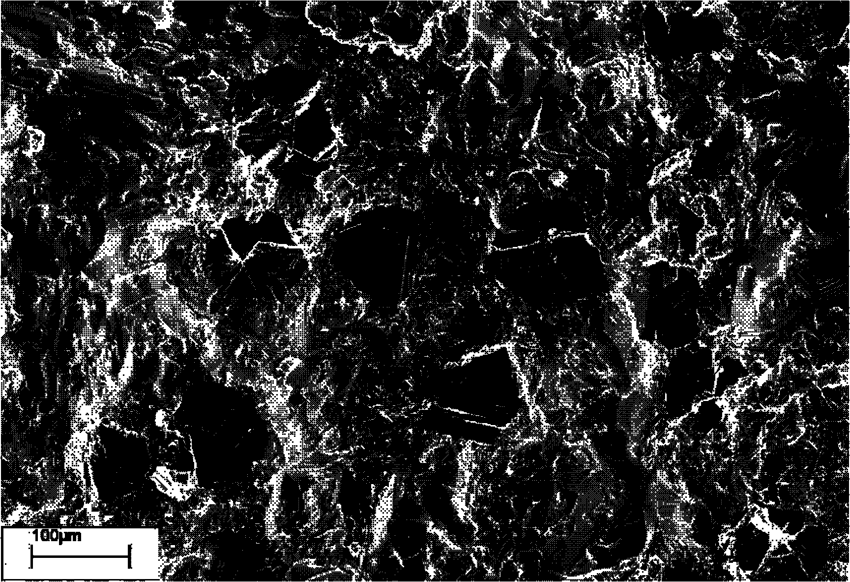
Image

Examples
Embodiment 1
[0016] According to weight percentage, 15% of adhesive phenolic resin, 10% of graphite, 25% of silicon powder with a particle size of -300 mesh, and 50% of diamond particles with a particle size of -100 mesh were wet mixed for 20 hours. Then, the composite blank was obtained by warm pressing at 50MPa pressure and 100°C temperature. Sintered at 1050°C for 24 hours in an argon protective atmosphere, and the density was 3.23g / cm2 after cooling with the furnace. 3 diamond / silicon / carbon porous substrate.
[0017] The prepared diamond / silicon / carbon porous matrix was placed in a graphite crucible, filled with liquid-phase infiltrated pure silicon, and then placed in a high-vacuum sintering furnace for vacuum liquid-phase infiltration for 0.5h, and the infiltration temperature was 1500°C , Vacuum degree -0.01MPa. After cooling with the furnace, a diamond-silicon carbide electronic packaging material with a density of 99.8% can be obtained.
Embodiment 2
[0019] According to weight percentage, 15% of adhesive phenolic resin, 5% of graphite, 20% of silicon powder with a particle size of -300 mesh, and 60% of diamond particles with a particle size of -500 mesh were wet mixed for 16 hours. Then, the composite blank was obtained by warm pressing under 10MPa pressure and 150°C temperature. Sintered at 1000°C for 24 hours in an argon protective atmosphere, and the density was 3.56g / cm2 after cooling with the furnace. 3 diamond / silicon / carbon porous substrate.
[0020] The prepared diamond / silicon / carbon porous matrix was placed in a graphite crucible, filled with liquid-phase infiltrated pure silicon, and then the whole was placed in a high-vacuum sintering furnace for vacuum liquid-phase infiltration for 1 hour, and the infiltration temperature was 1450°C. Vacuum degree -0.01MPa. After cooling with the furnace, a diamond-silicon carbide electronic packaging material with a density of 99.9% can be obtained.
Embodiment 3
[0022] According to weight percentage, 10% of adhesive phenolic resin, 10% of graphite, 20% of silicon powder with a particle size of -300 mesh, and 60% of diamond particles with a particle size of -500 mesh were wet mixed for 24 hours. Then, the composite blank was obtained by warm pressing under 30MPa pressure and 150°C temperature. Sintered at 1100°C for 24 hours in an argon protective atmosphere, and the density was 3.46g / cm2 after cooling with the furnace. 3 diamond / silicon / carbon porous substrate.
[0023] The prepared diamond / silicon / carbon porous matrix was placed in a graphite crucible, filled with liquid-phase infiltrated pure silicon, and then the whole was placed in a high-vacuum sintering furnace for vacuum liquid-phase infiltration for 0.5h, and the infiltration temperature was 1550°C , Vacuum degree -0.08MPa. After cooling with the furnace, a diamond-silicon carbide electronic packaging material with a density of 99.3% can be obtained.
PUM
| Property | Measurement | Unit |
|---|---|---|
| Density | aaaaa | aaaaa |
| Density | aaaaa | aaaaa |
| Density | aaaaa | aaaaa |
Abstract
Description
Claims
Application Information