Plasmon-enhancement-based quantum well infrared detector and preparation method thereof

A technology of infrared detectors and quantum wells, applied in semiconductor devices, final product manufacturing, sustainable manufacturing/processing, etc., can solve problems such as low coupling efficiency, achieve enhanced sensitivity, reduce the influence of noise signals, good contact characteristics and Effect of current spreading capability

Inactive Publication Date: 2013-08-07
SUZHOU INST OF NANO TECH & NANO BIONICS CHINESE ACEDEMY OF SCI
View PDF0 Cites 0 Cited by
  • Summary
  • Abstract
  • Description
  • Claims
  • Application Information

AI Technical Summary

Problems solved by technology

The traditional two-dimensional grating coupling method uses the refraction and diffraction of the incident light at the grating structure to obtain the electric field intensity parallel to the quantum well growth direction, and its coupling efficiency is still low

Method used


Image

  • Plasmon-enhancement-based quantum well infrared detector and preparation method thereof
  • Plasmon-enhancement-based quantum well infrared detector and preparation method thereof

Examples


Embodiment 1

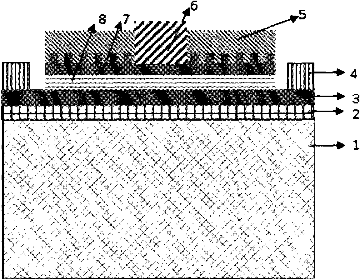
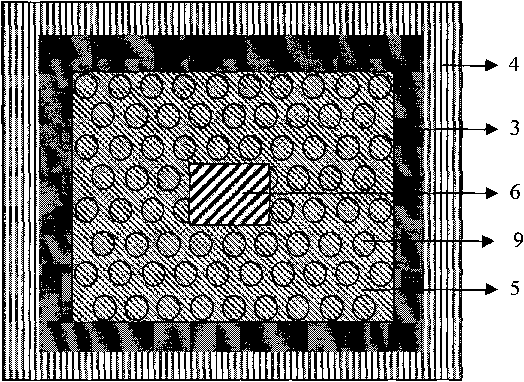
[0030] figure 1 It is a cross-sectional view of the device structure of Embodiment 1 of the present invention. figure 2 It is a top view of the device structure of Embodiment 1 of the present invention. As shown in the figure, 1 is a Si-GaAs substrate with a thickness of about 0.5mm; 2 is an AlAs buffer layer with a thickness of about 200nm; 3 is an AlGaAs:Si lower contact layer with a thickness of about 1000nm; 4 is a ring-shaped lower electrode. 5 is a metal thin film with a thickness of about 120nm, 6 is an upper electrode, 7 is an AlGaAs:Si upper contact layer with a thickness of about 2000nm, and 8 is a multi-quantum well layer, which is 50 cycles of AlGaAs / GaAs, that is, on the base material A layer of AlGaAs of tens of nanometers and a layer of GaAs of several nanometers are grown sequentially, and this cycle is repeated for 50 cycles, and 9 is the hole on the metal grating. The metal thin film 5 has a grating structure, the upper electrode 6 is embedded in the metal...

Embodiment 2

[0041] This embodiment is similar to the first embodiment, the only difference is that the material of the metal thin film is Ag, and the array of the metal grating structure is arranged in a square. The square arrangement also has its advantages, its arrangement is along the x and y axis, its arrangement is equivalent in both directions, and therefore its calculation is also equivalent.

Embodiment 3

[0043] This embodiment is similar to the first embodiment, and the only difference is that Al is used as the material of the metal thin film.


PUM


Abstract

The invention discloses a Plasmon-enhancement-based quantum well infrared detector and a preparation method thereof. The detector comprises a Si-GaAs substrate, an AlAs buffering layer, an AlAs:Si lower contact layer positioned on the buffering layer, a multi-quantum well layer, an AlAs:Si upper contact layer positioned on the multi-quantum well layer, a metal film, an upper electrode and an annular lower electrode, wherein the AlAs buffering layer is positioned on the substrate; the multi-quantum well layer is positioned on the AlAs:Si lower contact layer; the metal film and the upper electrode are positioned on the AlAs:Si upper contact layer; the metal film has a grating structure; the upper electrode is embedded in the metal grating structure; and the annular upper electrode is positioned on the lower contact layer and winds around the metal film, the upper contact layer and the multi-quantum well layer. In the detector, through the local area characteristic of Plasmon and the frequency-selecting characteristic of a raster, signals are enhanced and filtered, the absorption efficiency of a quantum well is improved, and the sensitivity of the quantum well infrared detector is increased.

Description

technical field [0001] The invention relates to the field of infrared photodetectors, in particular to a quantum well infrared detector based on Plasmon enhancement and a preparation method thereof. Background technique [0002] The quantum well infrared detector (Quantum Well Infrared Photodetector-QWIP) can artificially cut the bandgap width by changing the potential well width and barrier height, so as to realize the controllable response wavelength. And because of its mature material growth and preparation process, it is easy to integrate large area arrays, has good stability, good device uniformity, high number of operable pixels, high output, low cost, narrow spectral response bandwidth of detectors, and optical Small crosstalk, easy to realize two-color or multi-color focal plane devices, anti-radiation and most of the device technology can be compatible with HgCdTe infrared focal plane detectors, etc., in national defense detection, mineral resource detection, forest...

Claims


Application Information

Patent Timeline
Patent Type & Authority Patents(China)
IPC IPC(8): H01L31/101H01L31/0352H01L31/18
CPCY02P70/50
Inventor 李海军刘冬杨乐臣付凯王逸群
Owner SUZHOU INST OF NANO TECH & NANO BIONICS CHINESE ACEDEMY OF SCI
Why Eureka
Try Eureka