Light-emitting device package component

A technology for light-emitting devices and packaging components, which is applied to electrical components, electrical solid-state devices, semiconductor devices, etc., can solve the problems of decreased heat dispersion efficiency, the chip area occupied by electrodes 10, and the reduction of the total chip area, and achieves the effect of high heat dissipation capacity.

Active Publication Date: 2011-09-21
EPISTAR CORP
View PDF4 Cites 9 Cited by
  • Summary
  • Abstract
  • Description
  • Claims
  • Application Information

AI Technical Summary

Problems solved by technology

However, the gold wire 12 extends to the necessary length of the lead frame 6 so that the heat dissipation efficiency decreases
In add

Method used


Image

  • Light-emitting device package component
  • Light-emitting device package component
  • Light-emitting device package component

Examples


Embodiment Construction

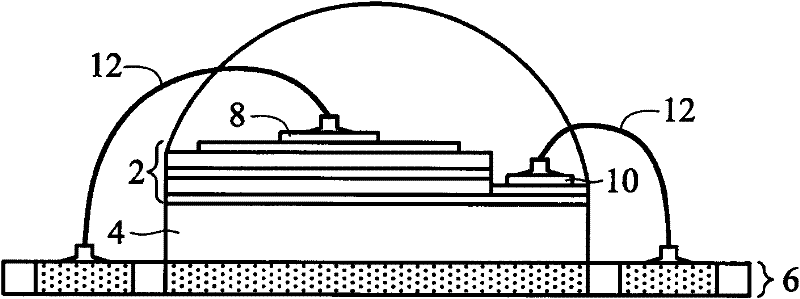
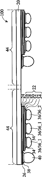
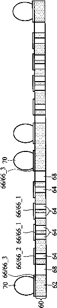
[0047] The present invention provides a novel light-emitting device (light-emitting device, LED) package component (package component) and a forming method thereof. Here, an example of an intermediate stage of the process is disclosed, followed by a discussion of different examples. In different views and illustrated embodiments, similar numerals are used to designate similar elements.

[0048] figure 2 A wafer 100 is disclosed that includes light emitting devices (LEDs) 22 formed on a substrate 20 . In one embodiment, the substrate 20 is made of sapphire (transparent aluminum oxide (Al 2 o 3 )), it can also be formed of other materials close to the characteristics of each layer in the light emitting device (LED) 22 (may include the third and fifth group elements or known compound semiconductor materials of the III-V group). The substrate 20 can also be a silicon carbide substrate, a silicon substrate with a silicon carbide layer thereon, a silicon germanium substrate or ...


PUM


Abstract

A light-emitting device (LED) package component includes an LED chip and a carrier chip. The carrier chip includes a first and a second bond pad on a surface of the carrier chip; and a third and a fourth bond pad on the surface of the carrier chip and electrically connected to the first and the second bond pads, respectively. The first, the second, the third, and the fourth bond pads are on a same surface of the carrier chip. The LED package component further includes a first and a second metal bump bonding the first and the second bond pads, respectively, onto the LED chip through flip-chip bonding; and a window-type module substrate bonded onto the third and the fourth bond pads through flip-chip bonding. The window-type module substrate includes a window, with the LED chip configured to emit light toward the window. The heat radiation performance is high and the light-emitting device package having a low thermal conductivity material is improved over conventional LED packages.

Description

technical field [0001] The invention relates to a light emitting device (LED) packaging component, in particular to a light emitting device (LED) packaging component including a through-substrate via (TSV). Background technique [0002] In recent years, the use of optical devices such as light emitting diodes (LEDs), laser diodes, and ultraviolet (UV) photodetectors has increased. Group-III nitride compounds such as gallium nitride (GaN) and related alloys are known to be suitable for the formation of optical devices. The wide bandgap and high electron saturation velocity of group III nitride compounds also make them excellent candidates for high-temperature and high-speed power electronic devices. [0003] Obtaining gallium nitride (GaN) host crystals is extremely difficult due to the high equilibrium pressure of nitrogen at typical growth temperatures. Therefore, GaN layers and respective light emitting diodes (LEDs) are usually formed on other substrates that can match ...

Claims


Application Information

Patent Timeline
IPC IPC(8): H01L33/62H01L33/64
CPCH01L33/58H01L2224/13H01L2224/48091H01L2224/49107H01L2224/8592H01L2224/45144H01L2924/00014H01L2924/00
Inventor 王忠裕
Owner EPISTAR CORP
Why Eureka
Try Eureka