Platform system for realizing circuit verification of Nandflash flash memory controller based on FPGA (Field Programmable Gate Array) and method thereof

A flash memory controller and controller technology, applied in static memory, instruments, etc., can solve the problems of low test efficiency, increased research and development costs, and inability to verify the logical function of Nandflash controller circuits, etc., to achieve stable and reliable work performance and a high degree of automation , the effect of shortening the R & D cycle

Inactive Publication Date: 2011-09-28
SHANGHAI MOBILEPEAK SEMICON
View PDF4 Cites 36 Cited by
  • Summary
  • Abstract
  • Description
  • Claims
  • Application Information

AI Technical Summary

Problems solved by technology

[0013] As mentioned above, the operation of the Nandflash controller is complicated. At the same time, there are various types of Nandflash flash memory chips in the market, and the differences are also increasing. The existing Nandflash controller FPGA verification scheme is increasingly difficult to meet the testing requirements of testers.
[0014] The Nandflash controller verification scheme in the prior art cannot fully verify the compatibility of the Nandflash controller to various Nandflash flash memory chips; becau

Method used


Image

  • Platform system for realizing circuit verification of Nandflash flash memory controller based on FPGA (Field Programmable Gate Array) and method thereof
  • Platform system for realizing circuit verification of Nandflash flash memory controller based on FPGA (Field Programmable Gate Array) and method thereof
  • Platform system for realizing circuit verification of Nandflash flash memory controller based on FPGA (Field Programmable Gate Array) and method thereof

Examples


Embodiment Construction

[0050] In order to understand the technical content of the present invention more clearly, the following examples are given in detail.

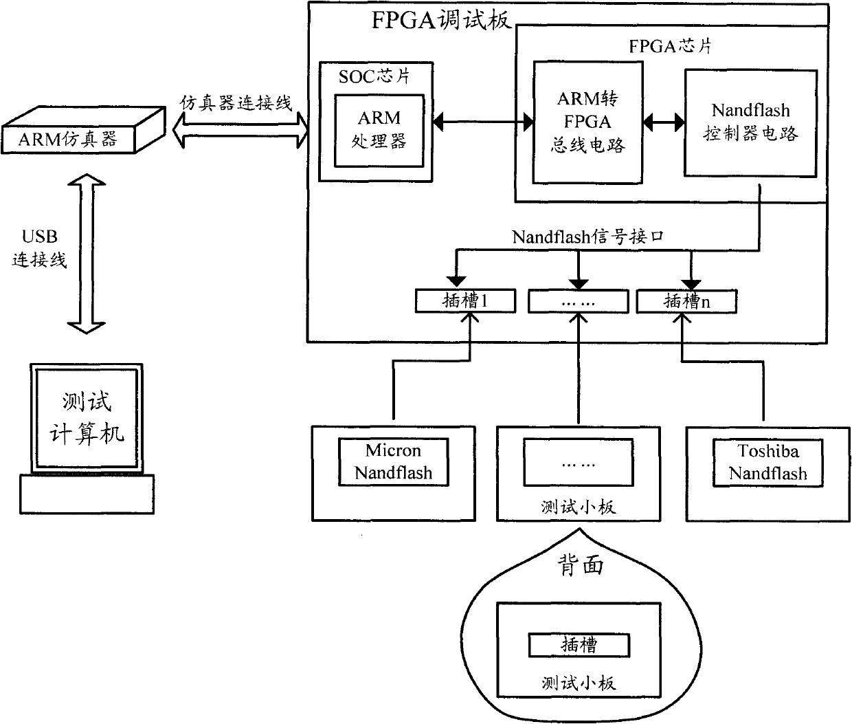
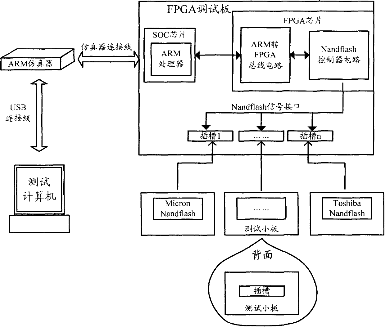
[0051] see figure 1 Shown, this platform system that realizes Nandflash flash memory controller circuit verification based on FPGA includes test computer and the test board that carries Nandflash flash memory chip, wherein, also includes test emulator and FPGA debugging board in the described platform system, described SOC chip, FPGA chip and several Nandflash signal interface modules are carried on the FPGA debugging board, bus conversion circuit module and Nandflash controller circuit module are arranged in the described FPGA chip, and described test computer passes through described test successively The emulator, the SOC chip, the bus conversion circuit module and the Nandflash controller circuit module are respectively connected with each of the Nandflash signal interface modules, and each Nandflash signal interface module is connected ...


PUM


Abstract

The invention relates to a platform system for realizing circuit verification of a Nandflash flash memory controller based on an FPGA (Field Programmable Gate Array). An FPGA debugging plate is provided with an SOC (System on Chip) chip, an FPGA chip and a plurality of Nandflash signal interface modules, the FPGA chip is provided with a bus switching circuit module and an Nandflash controller circuit module, a computer to be tested is connected with each Nandflash signal interface module through a test simulator, the SOC chip, the bus switching circuit module and the Nandflash controller circuit module, and each Nandflash signal interface module is connected with a corresponding test board. The invention further relates to a method for realizing the circuit verification of the Nandflash flash memory controller through the platform system. By adopting the platform system for realizing the circuit verification of the Nandflash flash memory controller based on the FPGA (Field Programmable Gate Array) and the method thereof, disclosed by the invention, the degree of automation is extremely high, the period of research and development is shortened, the cost of research and development is reduced, the test efficiency is high, the use is convenient and fast, the working performance is stable and reliable and the application range is wider.

Description

technical field [0001] The invention relates to the field of integrated circuits, in particular to the technical field of verification of digital integrated circuits, and specifically refers to a platform system and method for realizing circuit verification of Nandflash flash memory controllers based on FPGA. Background technique [0002] FPGA (Field Programmable Gate Array, Field Programmable Gate Array) verification is an essential and important process in the digital integrated circuit design process. [0003] The main steps of FPGA verification are: [0004] (1) Design input: use HDL (Hardware Description Language, hardware description language) input tools, schematic diagram input tools or state machine input tools to describe the circuit to be designed. [0005] (2) Synthesis and placement and routing, synthesis optimization is to translate HDL language into the most basic connection relationship (netlist) of NOR gates, and optimize the generated gate-level logic conn...

Claims


Application Information

Patent Timeline
IPC IPC(8): G11C29/56
Inventor 王冬佳张结华
Owner SHANGHAI MOBILEPEAK SEMICON
Why Eureka
Try Eureka