Organic electroluminescent device and manufacturing method thereof

An electroluminescent device and electroluminescent technology, which are applied in the fields of electro-solid devices, chemical instruments and methods, semiconductor/solid-state device manufacturing, etc. Hole balance, low electron injection barrier, effect of lowering injection barrier

Active Publication Date: 2011-10-05
KUNSHAN VISIONOX DISPLAY TECH +2
View PDF3 Cites 9 Cited by
  • Summary
  • Abstract
  • Description
  • Claims
  • Application Information

AI Technical Summary

Problems solved by technology

However, the preparation and storage of such active functional metals are difficult, and affect the preparation process of devices
Another way to improve the electron injection ability is to add an electron injection layer composed of an inorganic compound between the cathode and the organic layer. Practice has proved that LiF/Al is a cathode structure with excellent electron injection ab

Method used


Image

  • Organic electroluminescent device and manufacturing method thereof
  • Organic electroluminescent device and manufacturing method thereof
  • Organic electroluminescent device and manufacturing method thereof

Examples


Embodiment 1

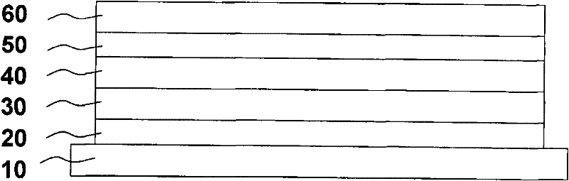
[0036] refer to figure 1 , is a cross-sectional view of the structure of the organic electroluminescent device of this embodiment, wherein the substrate 10, the anode layer 20, the hole transport layer 30, the light emitting layer 40, the cathode modification layer 50 and the cathode layer 60. The preparation structure of the organic electroluminescent device in the embodiment of the present invention is as follows:

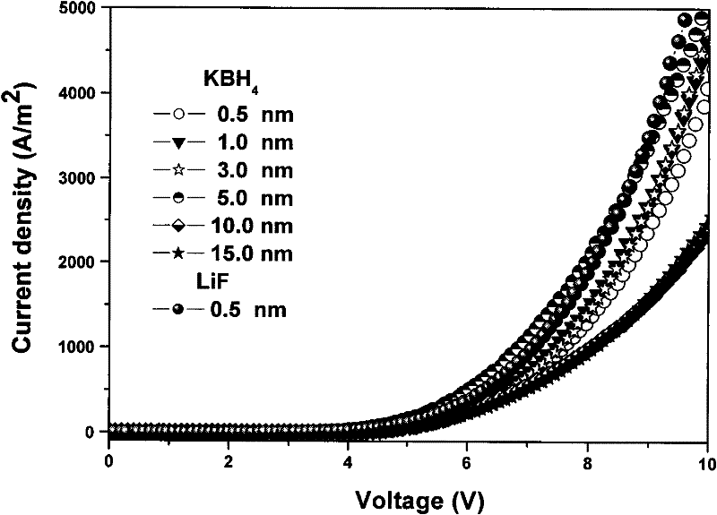
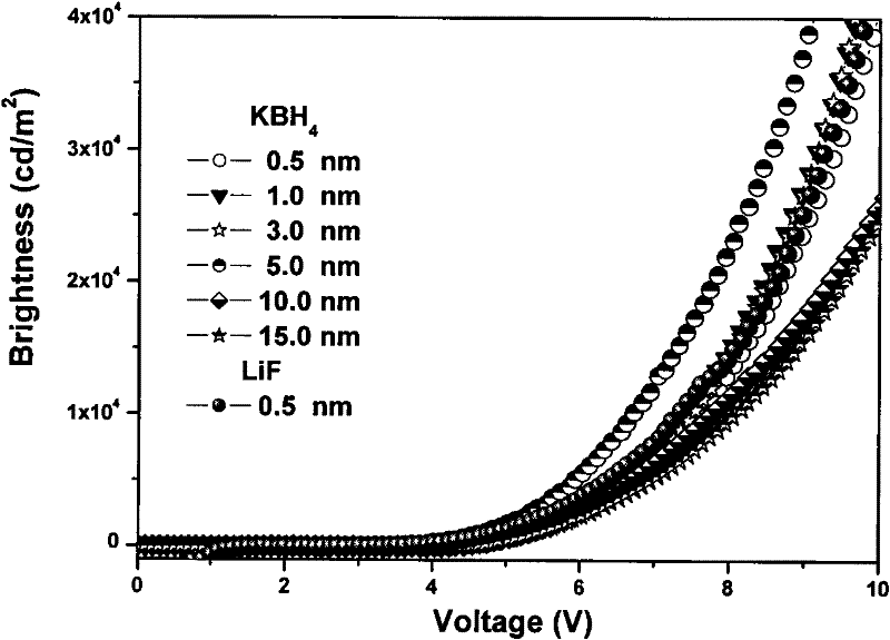
[0037] Glass substrate / ITO / NPB(50nm) / PADN: 1.5% C545T(30nm) / Alq 3 (30nm) / KBH 4 ((0.5nm) / Al(150nm)

[0038] 1) Preparation of organic light-emitting layer

[0039] Place the pretreated glass substrate in a vacuum chamber and evacuate to 1×10 -3 Pa, the hole transport material NPB is evaporated, the evaporation rate of the material film is 0.1nm / s, and the film thickness is 50nm to form a hole transport layer; 30nm thick PADN is sequentially evaporated on the hole transport layer: 1.5% C545T is used as the light-emitting layer of the device, and 30nm thick Alq...

Embodiment 2

[0047] The structural sectional view of the organic electroluminescent device of this embodiment is the same as that of Embodiment 1, such as figure 1 shown. The preparation structure of the organic electroluminescent device in the embodiment of the present invention is as follows:

[0048] Glass substrate / ITO / NPB(50nm) / PADN: 1.5% C545T(30nm) / Alq 3 (30nm) / KBH 4 ((1.0nm) / Al(150nm)

[0049] The preparation method is the same as in Example 1, except that the film thickness of the cathode modification layer in this example is 1.0 nm.

Embodiment 3

[0051] The structural sectional view of the organic electroluminescent device of this embodiment is the same as that of Embodiment 1, such as figure 1 shown. The preparation structure of the organic electroluminescent device in the embodiment of the present invention is as follows:

[0052] Glass substrate / ITO / NPB(50nm) / PADN: 1.5% C545T(30nm) / Alq 3 (30nm) / KBH 4 (3.0nm) / Al(150nm)

[0053] The preparation method is the same as in Example 1, except that the film thickness of the cathode modification layer in this example is 3.0 nm.


PUM

PropertyMeasurementUnit
Sheet resistanceaaaaaaaaaa
Film thicknessaaaaaaaaaa
Thicknessaaaaaaaaaa

Abstract

The invention discloses an organic electroluminescent device and a manufacturing method thereof. The organic electroluminescent device comprises a substrate, an anode layer, an organic functional layer and a cathode layer, wherein the anode layer is formed on the substrate; the organic functional layer is formed on the anode layer; the cathode layer is formed on the organic functional layer; a cathode modification layer containing No.I main group elements is also formed between the organic functional layer and the cathode layer; and the cathode modification layer is prepared from a compound which is directly decomposed into the No.I main group elements under the vacuum evaporation plating condition. In the invention, after a luminous layer is formed, the cathode modification layer is prepared; the electron injection capacity of a cathode interface is improved by the addition of the cathode modification layer, so that the performance of the device is obviously improved; meanwhile, in the preparing process, a material process has high feasibility, so that the yield of the device in the technological preparation process is further improved.

Description

technical field [0001] The invention relates to the field of organic electroluminescent devices, in particular to an organic electroluminescent device containing a cathode modification layer and a preparation method thereof. Background technique [0002] As early as the 1950s, Bernanose.A et al. started research on organic electroluminescent devices (OLEDs). The material initially studied was anthracene single crystal. Due to the problem that the thickness of the single crystal is too thick (10-20μm), the required driving voltage is very high (hundreds of volts). In 1982, Vinceet made a 50nm-thick anthracene film by vacuum evaporation, and observed blue fluorescence at 30 volts, but its external quantum efficiency was only 0.03%. Early organic electroluminescence hovered at the level of high voltage, low brightness, and low efficiency. Until 1987, Deng Qingyun (C.W.Tang) and Vanslyke of Eastman Kodak Company in the United States reported the structure as: ITO / Diamine / Alq ...

Claims


Application Information

Patent Timeline
IPC IPC(8): C09K11/06H01L51/54H01L51/56H01L51/50H01L27/32
Inventor 邱勇张国辉段炼董艳波
Owner KUNSHAN VISIONOX DISPLAY TECH
Why Eureka
Try Eureka