Organic light emission diode and preparation method thereof

An electroluminescence device and luminescence technology, applied in the field of electric light sources, can solve the problems of limited blocking effect, long diffusion distance, affecting the light efficiency and life of the device, etc., achieve a high qualified rate of finished products, reduce production costs, and improve production efficiency Effect

Inactive Publication Date: 2014-12-03
OCEANS KING LIGHTING SCI&TECH CO LTD +2
View PDF3 Cites 7 Cited by
  • Summary
  • Abstract
  • Description
  • Claims
  • Application Information

AI Technical Summary

Problems solved by technology

For example, the use of PN-doped transport layer technology can reduce the start-up voltage of OLED devices to improve light efficiency, and is conducive to the extension of life, but there are also problems: the thermal stability of P dopants such as F4-TCNQ is relatively poor, During the use of OLED devices, the doping structure itself is unstable, especially for the N doping of the electron transport layer, which is usually doped with alkali metal compounds, but due to the small volume of alkali metal ions, the diffusion ability Strong, the diffusion distance in the organic layer is long, the alkali metal ions will not only diffuse in the transport layer, but also diffuse into the light-emitting layer, directly leading to the quenching of excitons, affecting the light efficiency and life of the devi

Method used


Image

  • Organic light emission diode and preparation method thereof
  • Organic light emission diode and preparation method thereof
  • Organic light emission diode and preparation method thereof

Examples


preparation example Construction

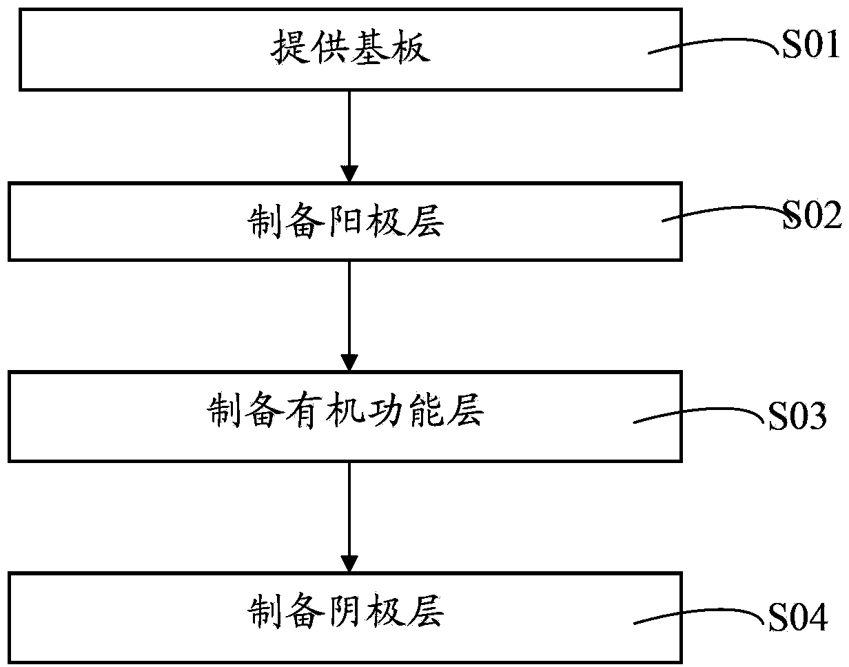
[0048] Correspondingly, the embodiment of the present invention also provides a preparation method of the above organic electroluminescent device. The process flow chart of the method is as image 3 Therefore, see also Figure 1~2 , the method includes the following steps:

[0049] S01. Provide the substrate 1;

[0050] S02. Prepare the anode layer 2: in a vacuum system, magnetron sputtering the transparent conductive oxide on the surface of the substrate 1 in step S01 to prepare the anode layer 2;

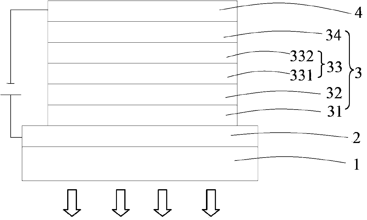
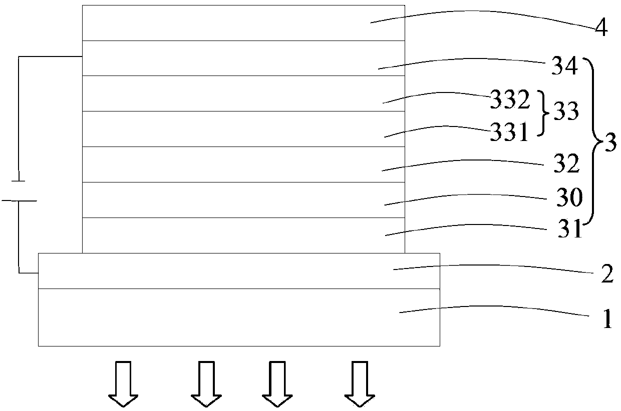
[0051] S03. Preparation of organic functional layer 3: In step S02, the surface of the anode layer 2 opposite to the surface of the light-transmitting substrate layer 1 is prepared by sequentially vapor-depositing the hole transport layer 31, the light-emitting layer 32, the n-doped barrier layer 33 and the electron transport layer. Layer 34, forming an organic functional layer 3;

[0052] S04. Prepare the cathode layer 4: In the vacuum coating system, the cathode layer 4 is f...

Embodiment 1

[0067] An organic electroluminescent device, its structure is: glass substrate / ITO(100nm) / F6-TNAP:MeO-TPD(1%, 60nm) / TAPC(10nm) / Ir(ppy) 3 :TPBi(8%,15nm) / BAlq(5nm) / BAlq:CsN 3 (1%,5nm) / CsN 3 :Bphen(15%,40nm) / Ag(100nm).

[0068] The preparation method of the organic electroluminescence device comprises the following steps:

[0069] 1) Pre-treatment of glass substrates: ultrasonically clean the glass substrates in deionized water containing detergent, after cleaning, ultrasonically treat them in isopropanol and acetone for 20 minutes, and then dry them with nitrogen to obtain a clean transparent substrate;

[0070] 2) Preparation of anode layer: In a vacuum system, magnetron sputtering of transparent conductive oxide ITO is formed on one side of the glass substrate pre-treated in step 1) to form an anode layer. The thickness of the anode layer is 100nm, and then the anode layer is formed The layered glass substrate is placed in a plasma treatment chamber for plasma treatment;

...

Embodiment 2

[0081] An organic electroluminescence device, its structure is: glass substrate / IZO (70nm) / MoO 3 :2-TNATA(10%,30nm) / TAPC(5nm) / Ir(piq) 3 :NPB(20%,20nm) / Gaq 3 (10nm) / Gaq 3 :LiN 3 (0.5%,5nm) / LiN 3 :TPBi(5%,30nm) / Al(70nm).

[0082] Its preparation method is with embodiment 1.


PUM

PropertyMeasurementUnit
Thicknessaaaaaaaaaa
Thicknessaaaaaaaaaa

Abstract

The invention discloses an organic light emission diode and a preparation method thereof. The organic light emission diode comprises a substrate, an anode layer, an organic function layer and a cathode layer which are in stack combination in sequence. The organic function layer comprises a hole transfer layer, a light-emitting layer, an organometallic complex barrier layer, an n-dopant-doped organometallic complex barrier layer and an electron transfer layer which are in stack combination in sequence. A preparation method comprises the steps of providing the substrate, preparing the anode layer, preparing the organic function layer comprising the n-dopant-doped barrier layer, and preparing the cathode layer and the like. The organic light emission diode has excellent use stability, long service life, and excellent luminous efficiency; the process is simple and easy to control the condition; the qualified rate of the finished product is high; the production efficiency is improved effectively; the production cost is reduced; and the organic light emission diode and the preparation method are suitable for industrialized production.

Description

technical field [0001] The invention belongs to the technical field of electric light sources, and in particular relates to an organic electroluminescent device and a preparation method thereof. Background technique [0002] Organic Light Emission Diode (hereinafter referred to as OLED) is a current-mode semiconductor light-emitting device based on organic materials. Its typical structure is to make a layer of tens of nanometers thick organic light-emitting material on the ITO glass as the light-emitting layer, and there is a metal electrode with a low work function above the light-emitting layer. [0003] The principle of OLED light emission is based on the action of an external electric field, electrons are injected from the cathode to the lowest unoccupied molecular orbital (LUMO) of organic matter, and holes are injected from the anode to the highest occupied orbital (HOMO) of organic matter. Electrons and holes meet, recombine, and form excitons in the light-emitting l...

Claims


Application Information

Patent Timeline
IPC IPC(8): H01L51/50H01L51/54H01L51/56
CPCH10K85/624H10K85/30H10K50/18H10K2102/00H10K71/00
Inventor 周明杰王平冯小明陈吉星
Owner OCEANS KING LIGHTING SCI&TECH CO LTD
Why Eureka
Try Eureka