Electronic packing method of vertical chips
An electronic packaging and chip technology, applied in the direction of circuits, electrical components, electrical solid devices, etc., can solve the problems of large size and unfavorable automatic production, etc., achieve good adaptability, reduce packaging costs, and improve packaging yield.
- Summary
- Abstract
- Description
- Claims
- Application Information
AI Technical Summary
Problems solved by technology
Method used
Image

Examples
Embodiment 1
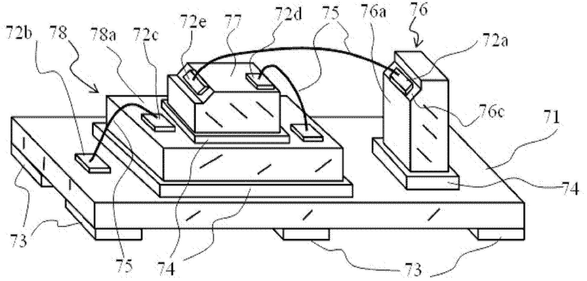
[0042] Such as figure 1 and Figure 7 As shown: in the packaging structure formed by the packaging method of the present invention, a bottom plate 71 is included, and a first vertical chip 76 is installed on the bottom plate 71 corresponding to the surface where the bottom plate lead solder bump 72b is arranged, and the first vertical chip 76 is bonded The body 74 is vertically installed on the base plate 71 , and the adhesive body 74 is adhesive or adhesive tape; specifically, the first vertical chip surface 76 a of the first vertical chip 76 is perpendicular to the base plate 71 . A first horizontal chip 77 and a second horizontal chip 78 are installed on the bottom plate 71, wherein the second horizontal chip 78 is mounted on the bottom plate 71 through the bonding body 74, and the first horizontal chip 77 is mounted on the second level through the bonding body 74. On the chip 78 , the surfaces of the first horizontal chip 77 and the second horizontal chip 78 are distribut...
Embodiment 2
[0048] Such as Figure 10As shown: only one chip is set on the base plate 71, the second vertical chip 87; that is, the second vertical chip surface 87a of the second vertical chip 87 is perpendicular to the base plate 71, and one end of the second vertical chip 87 is installed on the on the bottom plate 71. The second vertical chip 87 has a second vertical chip surface 87 a and a second vertical chip top side 87 c , the second vertical chip surface 87 a is a surface for fabricating functional devices, and the second vertical chip top side 87 c is parallel to the bottom plate 71 . Straight side lead solder bumps 72f are formed on the top side 87c of the second vertical chip, and the straight side lead solder bumps 72f are electrically connected to the electronic devices on the second vertical chip 87 . The straight side lead soldering block 72f is parallel to the bottom plate 71 , and the straight side lead soldering block 72f and the bottom plate lead soldering block 72b are...
Embodiment 3
[0057] Such as Figure 22 As shown: the fourth horizontal chip 94 is installed on the bottom plate 71 , the fourth horizontal chip 94 is distributed parallel to the bottom plate 71 , and the fourth horizontal chip 94 is installed on the bottom plate 71 through the bonding body 74 . A fourth vertical chip 98 is mounted on the bottom plate 71 , the fourth vertical chip surface 98 a of the fourth vertical chip 98 is perpendicular to the bottom plate 71 , and the fourth vertical chip 98 is mounted on the bottom plate 71 through the bonding body 74 . The fourth vertical chip 98 has a fourth vertical chip surface 98a, a fourth vertical chip vertical side 98b, and a fourth vertical chip top side 98c, wherein the fourth vertical chip vertical side 98b is adjacent to the end of the fourth horizontal chip 94; The vertical chip surface 98 a and the fourth vertical chip vertical side 98 b are both perpendicular to the bottom plate 71 , and the fourth vertical chip top side 98 c is paralle...
PUM
 Abstract
Description
Claims
Application Information
 - Generate Ideas
- Intellectual Property
- Life Sciences
- Materials
- Tech Scout
- Unparalleled Data Quality
- Higher Quality Content
- 60% Fewer Hallucinations
Browse by: Latest US Patents, China's latest patents, Technical Efficacy Thesaurus, Application Domain, Technology Topic, Popular Technical Reports.
© 2025 PatSnap. All rights reserved.Legal|Privacy policy|Modern Slavery Act Transparency Statement|Sitemap|About US| Contact US: help@patsnap.com