Method for texturing silicon wafer cut by diamond wire

A diamond wire cutting and silicon wafer technology, which is applied in chemical instruments and methods, final product manufacturing, sustainable manufacturing/processing, etc., can solve the problems of reducing the reflectivity of silicon wafers, low cutting process efficiency, waste mortar discharge and pollution of the environment, etc. , to achieve the effect of reducing reflectivity

Active Publication Date: 2011-10-19
TRINA SOLAR CO LTD
View PDF10 Cites 29 Cited by
  • Summary
  • Abstract
  • Description
  • Claims
  • Application Information

AI Technical Summary

Problems solved by technology

[0002] At present, multi-wire cutting machines are commonly used for cutting solar silicon wafers, and MB, HCT, NTC, etc. have a relatively large market share. However, due to the low efficiency of this cutting process, one cut takes 7 to 8 hours, and SiC and PEG mixed mortar, the discharge of waste mortar after cutting seriously pollutes the environment. In view of the above problems, a new cutting process has been developed internationally, diamond wire cutting, its cutting speed is 2 to 3 times that of ordinary wire cutting, and there is Need to use SiC, use water-based cutting fluid that is not polluting to the environment
However, due to the different cutting principles, the influence on the surface morphology of silicon wafers is also different. Compared with normal mortar cutting silicon wafers, the surface of silicon wafers obtained by diamond wire cutting technology is smoother and has fewer surface defects. figure 1 and 2
The acid texturing process is to use the defects on the surface of the silicon wafer to perform isotropic etching, thereby reducing the reflectivity of the silicon wafer. If the normal silicon wafer acid texturing process is HF-HNO 3 -H 2 O-acid texturing process, the silicon wafers obtained by diamond wire cutting have less surface defects, the ideal texture cannot be obtained after texturing, the reflectivity is much higher than the normal silicon wafer level, and its battery conversion efficiency is also relatively low, making this new type Cutting process silicon wafers cannot be mass-produced

Method used


Image

  • Method for texturing silicon wafer cut by diamond wire
  • Method for texturing silicon wafer cut by diamond wire
  • Method for texturing silicon wafer cut by diamond wire

Examples


Embodiment Construction

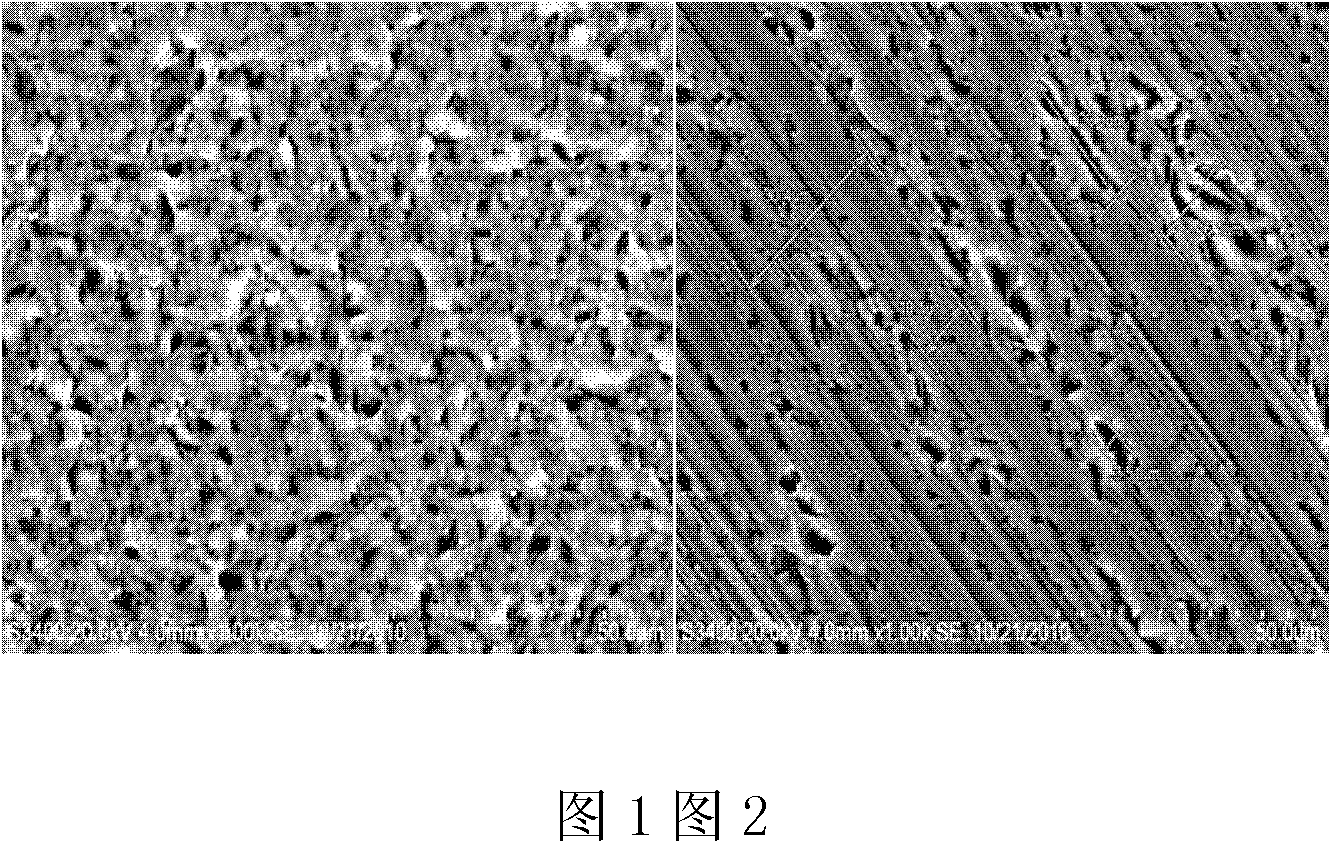
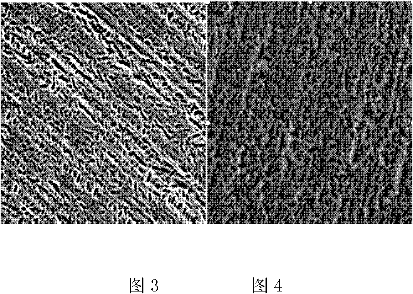
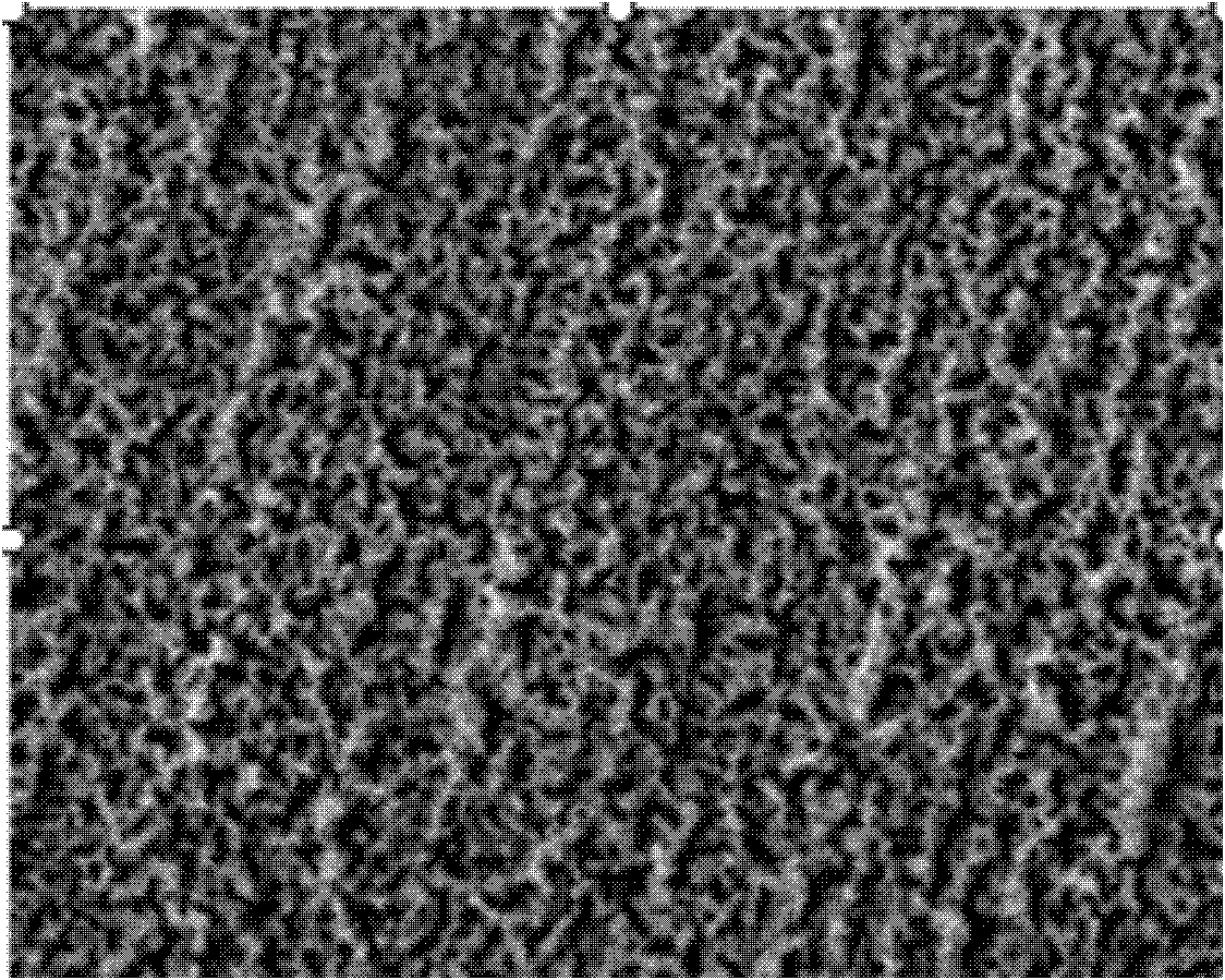
[0020] A method for making texture of a diamond wire cut silicon wafer, the production method is as follows:

[0021] (1) Thickness and fine cleaning of silicon wafers cut by diamond wire, and drying, sorting and packaging of silicon wafers after cleaning;

[0022] (2), the cleaned silicon wafer is in H 2 SO 4 or H 3 PO 4 -HF-HNO 3 The system undergoes acid corrosion reaction:

[0023] (3), the volume ratio of the acid in step (2) is: H 2 SO 4 or H 3 PO 4 :HF:HNO 3 =2-10:1-4:1-4, where H 2 SO 4 The weight percent concentration of HF is 98%, the weight percent concentration of HF is 49%, HNO 3 The weight percent concentration is 63%, H 3 PO 4 The weight percentage concentration is 85%, and the reaction time is 30-70s;

[0024] (4), above-mentioned silicon chip that has reacted with acid is soaked in 5% NaOH solution, reaction time 15s;

[0025] (5), soak the above-mentioned silicon chip reacted with alkali in the HCl-HF solution for 60s, then clean it with deion...


PUM

PropertyMeasurementUnit
reflectanceaaaaaaaaaa

Abstract

The invention belongs to the technical field of the texturing of silicon wafers, and particularly relates to a method for texturing a silicon wafer cut by a diamond wire, which comprises the following steps of: 1, cleaning the silicon wafer cut by the diamond wire; 2, performing acidic corrosion reaction on the cleaned silicon wafer in H2SO4 or H3PO4-HF-HNO3 mixed acidic solution for 30 to 70 seconds, wherein a volume ratio of the H2SO4 or the H3PO4 to the HF to the HNO3 is (2-10):(1-4):(1-4), the concentration of the H2SO4 is 98 percent, the concentration of the HF is 49 percent, the concentration of the HNO3 is 63 percent, and the concentration of the H3PO4 is 85 percent; 3, soaking the silicon wafer which reacts with the acids in alkali texturing liquid, and reacting for 10 to 30 seconds; 4, soaking the silicon wafer which reacts with alkali in HCL-HF solution for 30 to 120 seconds; and 5, drying the reacted silicon wafer, and performing subsequent cell process manufacturing. Compared with the conventional texturing process, the optimized method for texturing the silicon wafer cut by the diamond wire has the advantages that: the reflectivity of the textured silicon wafer is reduced by about 6 percent, and the cell efficiency is improved greatly.

Description

technical field [0001] The invention belongs to the technical field of silicon wafer texturing, in particular to a diamond wire-cut silicon wafer texturing method. Background technique [0002] At present, multi-wire cutting machines are commonly used for cutting solar silicon wafers, and MB, HCT, NTC, etc. have a relatively large market share. However, due to the low efficiency of this cutting process, one cut takes 7 to 8 hours, and SiC and PEG mixed mortar, the discharge of waste mortar after cutting seriously pollutes the environment. In view of the above problems, a new cutting process has been developed internationally, diamond wire cutting, its cutting speed is 2 to 3 times that of ordinary wire cutting, and there is It is necessary to use SiC and use water-based cutting fluid that is not polluting to the environment. However, due to the different cutting principles, the influence on the surface morphology of silicon wafers is also different. Compared with normal mor...

Claims


Application Information

Patent Timeline
Patent Type & Authority Applications(China)
IPC IPC(8): C30B33/10C23F1/24C23F1/40H01L31/18
CPCY02P70/50
Inventor 李毕武刘振淮黄振飞
Owner TRINA SOLAR CO LTD
Why Eureka
Try Eureka