Array substrate and liquid crystal display panel

A technology of array substrate and transparent substrate, applied in the field of liquid crystal display, can solve the problems of slow photocuring of sealant, reduced production efficiency, increased power consumption, etc., and achieves the effects of reducing production cost, improving production efficiency and increasing power consumption

Active Publication Date: 2011-10-19
KUSN INFOVISION OPTOELECTRONICS
View PDF2 Cites 8 Cited by
  • Summary
  • Abstract
  • Description
  • Claims
  • Application Information

AI Technical Summary

Problems solved by technology

In each "fan-shaped" connection area, the length of the wiring increases from the middle of the "fan-shaped" area to both sides, so that the resistance value (R) and coupling capacitance (C) of the wiring also increase from the middle of the "fan-shaped" area to the two sides. The two sides increase, so that the wiring has a different RC delay time, and the different RC delay time will cause the image quality of the liquid crystal display panel to degrade, such as the phenomenon of water ripples (mura). In order to make each wiring in the "sector" area have a For the same RC delay time, the current solution is to set one end of the wiring in the "sector" area or the wiring at the upper and lower ends as bent wiring, and compensate for the difference in length so that each wiring has a same RC delay time
figure 2 Yes figure 1 The enlarged view of the middle area 10, where the data lines 12 with periodically arranged square-wave bent wiring structure are coated with frame glue 3, the data lines 12 are essentially arranged along the longitudinal direction, and the frame glue 3 is cured by light In this case, since the data line 12 itself is opaque, it will block part of the light from passing through and affect the curing speed of the sealant 3
For example, in figure 2 The width of the horizontal narrow and long region 21 and the horizontal narrow and long region 22 is 1/4 period of the data line 12. However, since the horizontal narrow and long region 21 always has the short side of the square wave and bent trace, However, there is always a long side of a square-shaped bent line in the laterally long and narrow region 22, so it can be s

Method used


Image

  • Array substrate and liquid crystal display panel
  • Array substrate and liquid crystal display panel
  • Array substrate and liquid crystal display panel

Examples


no. 1 approach

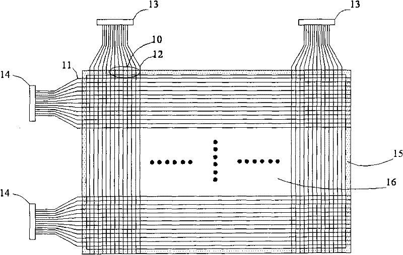
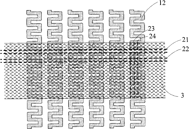
[0023] Figure 4 It is a partially enlarged schematic diagram of the wiring of the thin film transistor array substrate in the liquid crystal display panel according to the first embodiment of the present invention. A plurality of wirings are located under the frame glue 3, and the area covered by the frame glue 3 is the frame glue area. The multiple wirings can be scanning lines or data lines. All the following implementation methods will use the wiring as the data line 12 as an example. For detailed description, of course, the present invention is also applicable to the case where a plurality of wirings are scanning lines. Such as Figure 4 As shown, the plurality of wirings are data lines 12 . In the sealant area, any data line 12 among the multiple data lines 12 has a periodic wave bending pattern, the period of the wave bending pattern is T1, and the wave bending pattern is square in each period T1. Wavy zigzag pattern. The square-wave bending pattern of any data line...

no. 2 approach

[0027] The similarities between the second embodiment and the first embodiment will not be repeated. Figure 5 It is a partially enlarged schematic diagram of the wiring of the thin film transistor array substrate in the liquid crystal display panel according to the second embodiment of the present invention. Compared with the first embodiment, the second embodiment is different in that, in the second embodiment, the square-wave bending patterns between adjacent data lines 12 are arranged with a 3 / 4 cycle offset from each other, Figure 5 The arrangement of the even-numbered data lines 12 can be regarded as the result of the downward translation of the odd-numbered data lines 12 by 3 / 4 of the period of the square-wave bending pattern. Figure 5 Take the horizontal narrow and long regions 51 and 52 respectively, the width of which is 1 / 4 of the bending period of the square wave of the data line 12, and the length is the total length a of the frame glue in the transverse directi...

no. 3 approach

[0031] The difference between the third embodiment of the present invention and the above-mentioned first and second embodiments is that the first and second embodiments only consider making the light-receiving area of ​​the sealant uniform in the transversely long and narrow region perpendicular to the longitudinal extension direction of the data lines, The third embodiment comprehensively considers the longitudinally long and narrow areas along the longitudinal extension of the data lines and the transversely long and narrow areas perpendicular to the longitudinal extension of the data lines, so that the light-receiving area of ​​the frame glue is as uniform as possible.

[0032] The similarities between the third embodiment and the first and second embodiment will not be repeated. Figure 6 It is a partially enlarged schematic diagram of the wiring of the thin film transistor array substrate in the liquid crystal display panel according to the third embodiment of the present...


PUM


Abstract

The invention provides an array substrate and a liquid crystal display panel. The array substrate comprises a transparent substrate and a plurality of opaque distribution wires positioned on the transparent substrate; the plurality of distribution wires extend and pass through a frame glue area; random one of the plurality of distribution wires has periodical waveform bent patterns in the frame glue area; and the period of the waveform bent patterns of the distribution wires is staggered relative to the adjacent distribution wires. The liquid crystal display panel comprises the array substrate, an opposed substrate opposite to the array substrate and frame glue stuck between the two substrates; the frame glue is stuck to the frame glue area of the array substrate; the frame glue is sealedbetween the two substrates to form a display area; and a liquid crystal layer is filled in the display area. The frame glue is quickly cured without increasing the power consumption, so that the production efficiency is improved.

Description

【Technical field】 [0001] The invention relates to the field of liquid crystal display, in particular to an array substrate and a liquid crystal display panel with a special wiring structure. 【Background technique】 [0002] Liquid Crystal Display (LCD) has the advantages of good picture quality, small size, light weight, low driving voltage, low power consumption, no radiation and relatively low manufacturing cost, and currently occupies a dominant position in the field of flat panel display. Liquid crystal displays are ideally suited for use in desktop computers, palmtop computers, personal digital assistants (Personal Digital Assistant, PDA), cellular phones, televisions, and a variety of office automation and audio-visual equipment. [0003] The liquid crystal display panel is the main component of the liquid crystal display. The commonly used liquid crystal display panel is composed of a thin film transistor (Thin Film Transistor, TFT) array substrate, a color filter (Col...

Claims


Application Information

Patent Timeline
IPC IPC(8): G02F1/1362H01L27/12
Inventor 郑会龙简廷宪廖家德
Owner KUSN INFOVISION OPTOELECTRONICS
Why Eureka
Try Eureka