Graphical flexible transparent conductive film and preparation method thereof
A transparent conductive film and patterning technology, applied in the direction of transparent dielectric, conductive layer on insulating carrier, printed circuit manufacturing, etc. The effect of improving conductivity
- Summary
- Abstract
- Description
- Claims
- Application Information
AI Technical Summary
Problems solved by technology
Method used
Image
Examples
Embodiment 1
[0028] Embodiment 1: A transparent conductive film is made by combining grooves with equal hexagonal grooves as the basic unit
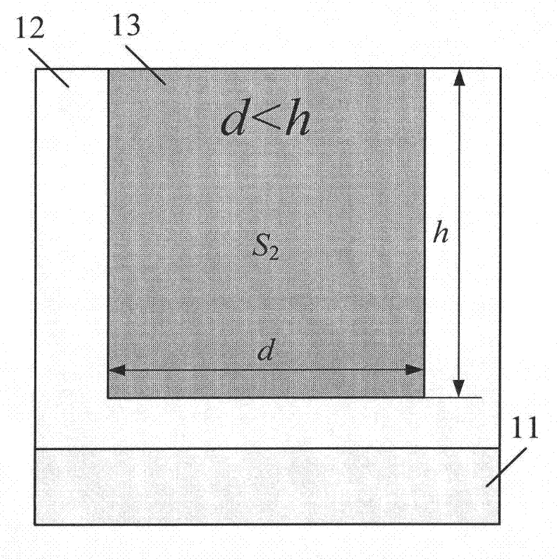
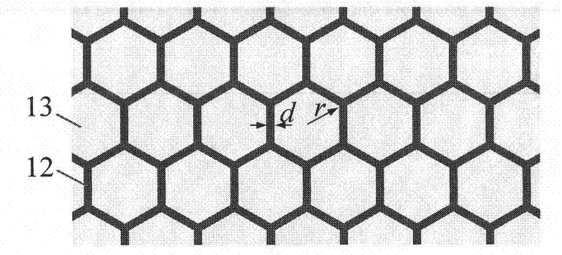
[0029] In this embodiment, the patterned flexible transparent conductive film, such as figure 2 with image 3 As shown, it includes a transparent and flexible substrate 11 , a transparent embossing glue 12 integrally bonded on the substrate 11 , and a conductive film 13 uniformly filled in the groove bottom of the transparent embossing glue 12 .
[0030] Wherein the transparent flexible substrate 11 is PET with a thickness of 100 μm. The transparent embossing glue 12 is a solvent-free UV-curable acrylic resin with a thickness of 5 μm. The groove network on the surface of the transparent embossing glue 12 is a hexagonal array, the radius of the circumscribed circle of the hexagon is r=5 μm, the value of the groove width d is 500nm~10 μm (preferably 1 μm in this embodiment), and the depth h=2 μm. The wall angle is about 82°. The conductive film 13...
Embodiment 2
[0036] Embodiment 2: A transparent conductive film is made by combining grooves with square grooves as the basic unit
[0037] In this embodiment, the patterned flexible transparent conductive film, such as Figure 5 As shown, it includes a transparent flexible substrate 11 , a transparent embossing glue 12 disposed above the substrate 11 , and a conductive film 13 uniformly filled in the groove bottom of the transparent embossing glue 12 .
[0038] Wherein the transparent flexible substrate 11 is PC with a thickness of 50 μm. The transparent embossing glue 12 is PMMA with a thickness of 6 μm. The groove network on the surface of the transparent embossing adhesive 12 is a square array, the side length of the square is 400 μm, the groove width d=10 μm, the depth h=11 μm, and the side wall angle is about 88°. The conductive film 13 after sintering is simple copper, and the copper is evenly filled in the bottom of the groove of the transparent embossing adhesive, and communicat...
PUM
| Property | Measurement | Unit |
|---|---|---|
| Thickness | aaaaa | aaaaa |
| Thickness | aaaaa | aaaaa |
| Thickness | aaaaa | aaaaa |
Abstract
Description
Claims
Application Information


