Light emitting diode and manufacturing method thereof

A technology of light-emitting diodes and manufacturing methods, which is applied in the direction of electrical components, electrical solid devices, circuits, etc., and can solve the problems of unsatisfactory light emitting angle, height and optical density of a single LED, high processing cost of a single SMD, and poor consistency of phosphor distribution And other problems, to achieve the effect of good macroscopic visual effect, good batch operation consistency, and good anti-UV performance

Inactive Publication Date: 2011-10-19
ZHUHAI LEADFULL OPTOELECTRONICS IND
View PDF4 Cites 2 Cited by
  • Summary
  • Abstract
  • Description
  • Claims
  • Application Information

AI Technical Summary

Problems solved by technology

[0004] 1. The process of adding aluminum frame to aluminum substrate is complicated and the material cost is expensive
[0005] 2. During the operation of semi-finished products, especially when packaging white light, due to the large number of chip particles and the excessive length of the aluminum substrate (more than 10mm), there are fatal flaws in the consistency of phosphor distribution
[0006] 3. During the operation of semi-finished products, when the aluminum substrate is baking fluorescent glue in an oven, it is very easy to be deformed at high temperature, which also leads to poor distribution of phosphor powder
[0009] 1. Single SMD and high processing cost
[0010] 2. When designing the finished product, the light emitting angle, height and optical density of a single LED cannot be perfect, which seriously affects the macroscopic visual effect
[0011] 3. Multiple SMDs are integrated with aluminum boards and PCBs, which also has high processing costs and dark areas between particles, which affect the macroscopic visual effect.

Method used


Image

  • Light emitting diode and manufacturing method thereof
  • Light emitting diode and manufacturing method thereof
  • Light emitting diode and manufacturing method thereof

Examples


Embodiment 1

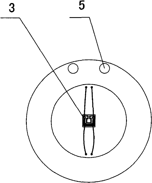
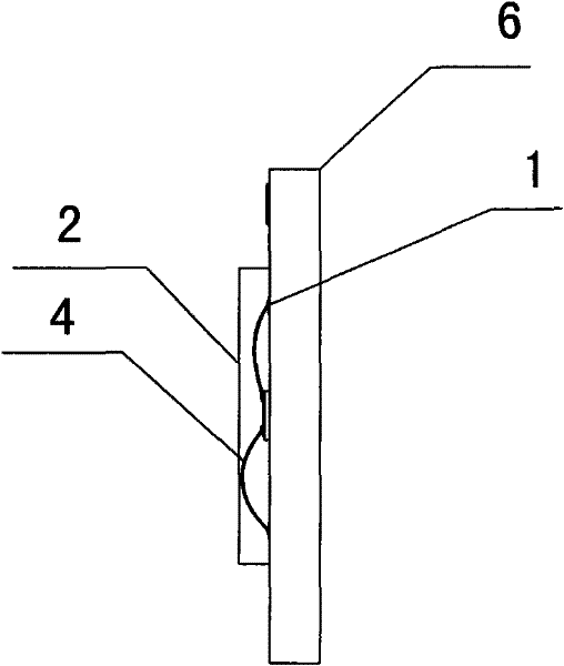
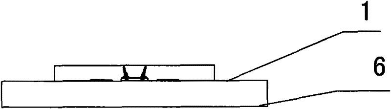
[0059] The invention discloses a light emitting diode, such as figure 1 , 2 , 3, including: an electrode set 1, a chip 3 installed on the front of the electrode set 1, a connection 4 and an electrode 5, wherein the light-emitting diode adopts a two-layer structure, and the electrode set 1 forms the light-emitting diode The first layer; the light-emitting diode also includes a rubber cake 2, the rubber cake 2 covers the front of the electrode set 1, and the chip 3, the wiring 4, and the electrode 5 are covered on the rubber cake 2 and the electrode set 1; the rubber cake 2 forms the second layer of the light emitting diode.

[0060] The COB series adopts a thermoelectric separation structure. The electrode set 1 is the frame of the LED light source device. The rubber cake 2, the chip 3, the connection line 4, the electrode 5, and the heat sink 6 are all fixed and installed through the electrode set 1.

[0061] The electrode assembly 1 includes a substrate, the front of the su...

Embodiment 2

[0080] Such as Figure 5 , in this embodiment, the light-emitting diode includes: an electrode set 1, a chip 3 installed on the front of the electrode set 1, a wire 4, and an electrode 5. The light-emitting diode adopts a two-layer structure, and the electrode set 1 forms the The first layer of the light-emitting diode; the light-emitting diode also includes a rubber cake 2, the rubber cake 2 covers the front of the electrode set 1, and the chip 3, the wiring 4, and the electrode 5 are covered on the rubber cake 2 Between the electrode assembly 1; the rubber cake 2 forms the second layer of the light-emitting diode; wherein, the light-emitting diode also includes a plurality of chips 3, and the plurality of chips 3 are spaced from each other and arranged on the front of the electrode assembly 1; Two or n groups of connecting wires 4 start from the electrodes on the plurality of chips 3 respectively, and respectively connect the chips 3 with the electrodes on the electrode set,...


PUM


Abstract

The invention provides a light emitting diode and a manufacturing method thereof. The light emitting diode is simple to manufacture, has good consistency in client use consistency and high yield, and the shape of the light emitting diode can be designed or changed arbitrarily. The technical scheme of the invention is that: the light emitting diode comprises an electrode kit, a chip installed on the front surface of the electrode kit, a connection wire and an electrode, wherein the light emitting diode has a two-layered structure; the electrode kit is formed on the first layer of the light emitting diode; the light emitting diode further comprises a rubber cake; the rubber cake covers the front surface of the electrode kit, and covers the chip, the connection wire and the electrode between the rubber cake and the electrode kit; and the rubber cake is formed on the second layer of the light emitting diode. The electrode kit comprises a substrate; the front surface of the substrate is provided with a chip bonding area; the chip is fixed in the chip bonding area; and the electrode kit further comprises a heat sink, and the hear sink is embedded in the back surface of the substrate.

Description

technical field [0001] The invention belongs to the technical field of light-emitting diodes, and in particular relates to a multi-functional, high-reliability light-emitting diode-COB series device suitable for the lighting market and a manufacturing method thereof. Background technique [0002] Light emitting diode (light emitting diode) abbreviation and commonly known as LED, is a semiconductor solid light emitting device. It uses a solid chip as a light-emitting material, recombines carriers in the semiconductor, and releases excess energy to cause photon emission, emitting red, yellow, blue, green, blue, orange, purple, and white visible or invisible light. Circuit symbol: LED light sources have developed rapidly in recent years, and the luminous efficiency has been continuously improved, reaching 120Lm / W. Therefore, LED has gradually entered the field of commercial lighting and general lighting. LED lighting reform will be the third historic lighting reform. Light-e...

Claims


Application Information

Patent Timeline
Patent Type & Authority Applications(China)
IPC IPC(8): H01L33/48H01L33/52H01L33/62H01L33/64
CPCH01L25/0753H01L2224/48091H01L2224/73265H01L2933/005
Inventor 林建明陈秀莲黄泽语
Owner ZHUHAI LEADFULL OPTOELECTRONICS IND
Why Eureka
Try Eureka