

Metallic wiring etching solution and metallic wiring forming method using the etching solution
A technology of metal wiring and etching solution, which is applied in the direction of chemical instruments and methods, luminescent materials, etc., can solve the problems of high price, stability, and change, and achieve the effects of reducing costs, ensuring process redundancy, and maintaining performance
- Summary
- Abstract
- Description
- Claims
- Application Information
AI Technical Summary
Problems solved by technology
Method used
Image

Examples
Embodiment
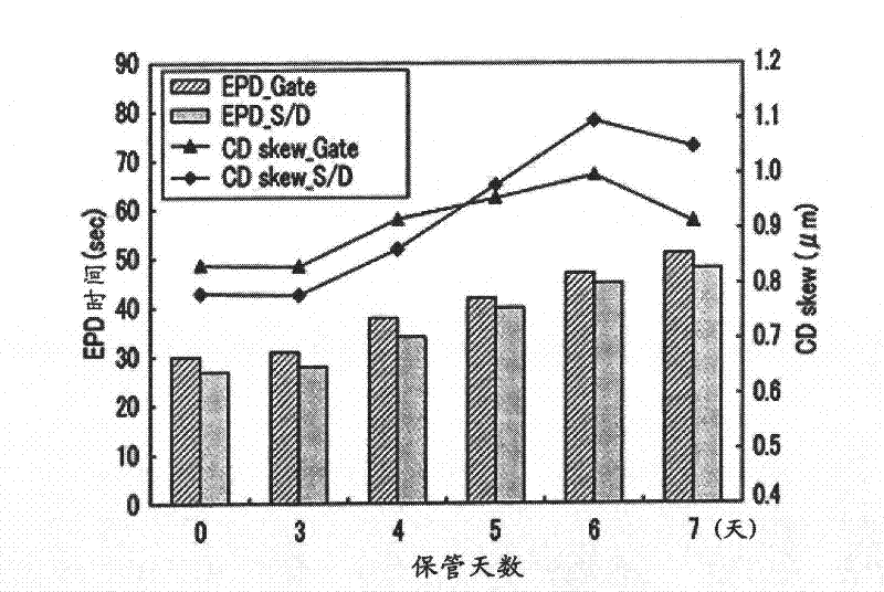
[0053] The metal wiring etching solution of the embodiment of the present invention comprises: ammonium persulfate, 0.1%-30% by weight of organic acid, 0.01%-5% by weight of phosphate, and azole compounds. In this etching solution, an organic acid was used instead of an inorganic acid, and a phosphate was added to the metal wiring etching solution of the comparative example.
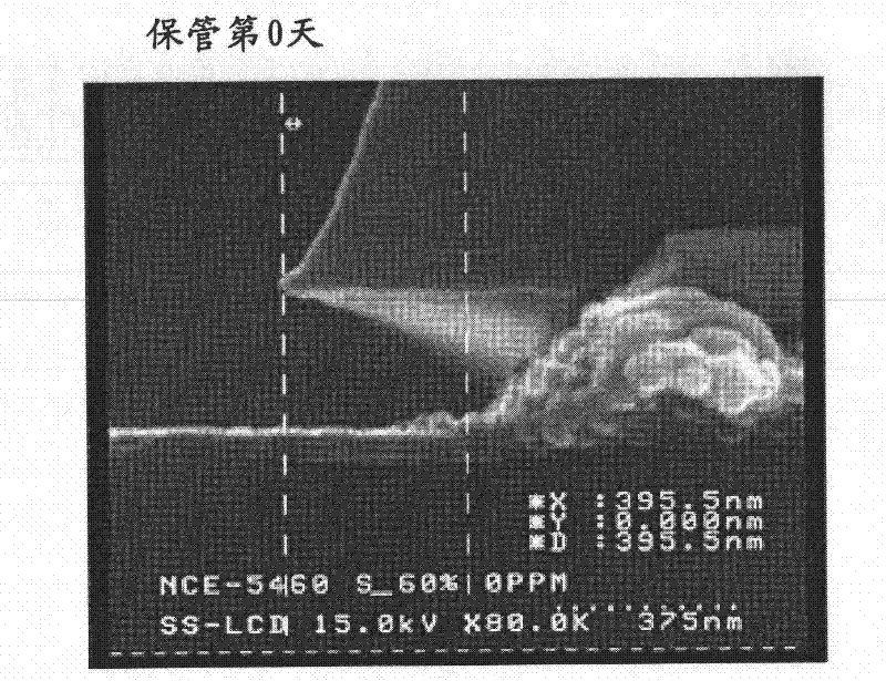
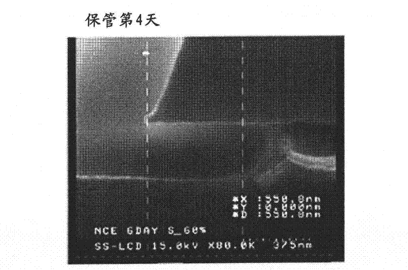
[0054] After forming a double layer of a titanium film and a copper film on a substrate and forming a photoresist pattern on the double layer, the double layer was etched using the etching solution. At this time, the processes are implemented respectively according to the substrate size (23 "and 40"). When the substrate size is 23 ", the thicknesses of the titanium film and the copper film are respectively formed as 300" 2000 When the substrate size is 40 ", the thickness of titanium film and copper film are respectively formed as 300 3000 The double layer is etched after being formed as source an...
PUM
 Abstract
Description
Claims
Application Information