A method for preparing cds/zns nanowire heterojunction

A nanowire and single-crystal nanotechnology, which is applied in the field of nano-heterojunction preparation, achieves the effect of uniform morphology, easy promotion, and short time-consuming

Inactive Publication Date: 2011-11-30
XINJIANG UNIVERSITY
View PDF5 Cites 4 Cited by
  • Summary
  • Abstract
  • Description
  • Claims
  • Application Information

AI Technical Summary

Problems solved by technology

At present, the methods of synthesizing CdS / ZnS nano-heterostructure products are mostly liquid phase method and chemical vapor deposition method, but there are no related reports on the preparation of CdS / ZnS nanowire heterojunction by vacuum thermal evaporation method.

Method used


Image

  • A method for preparing cds/zns nanowire heterojunction
  • A method for preparing cds/zns nanowire heterojunction
  • A method for preparing cds/zns nanowire heterojunction

Examples


Embodiment 1

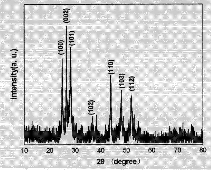
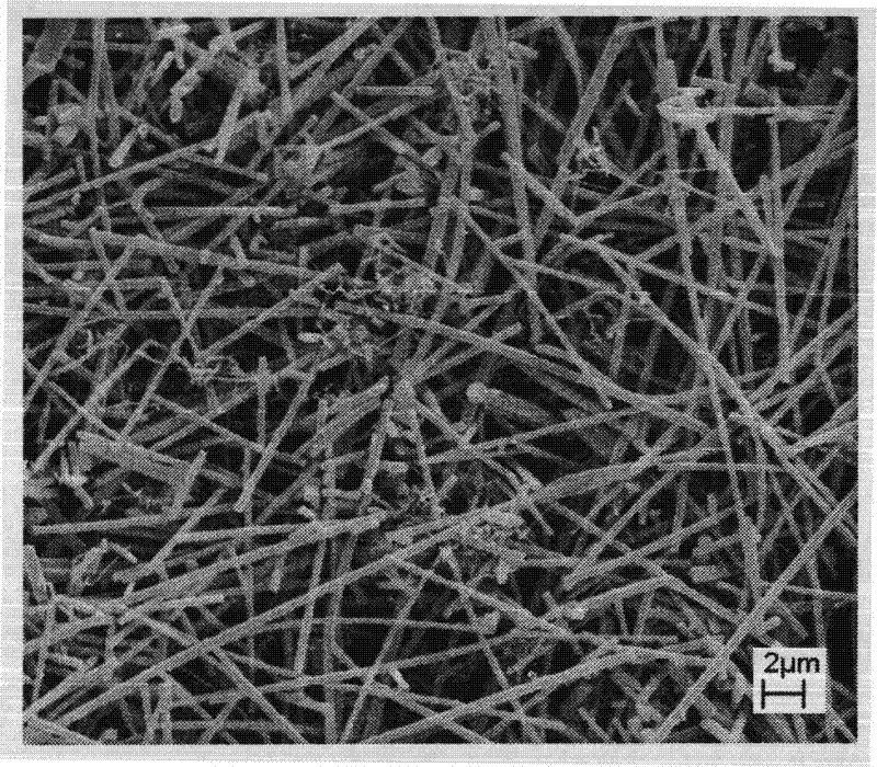
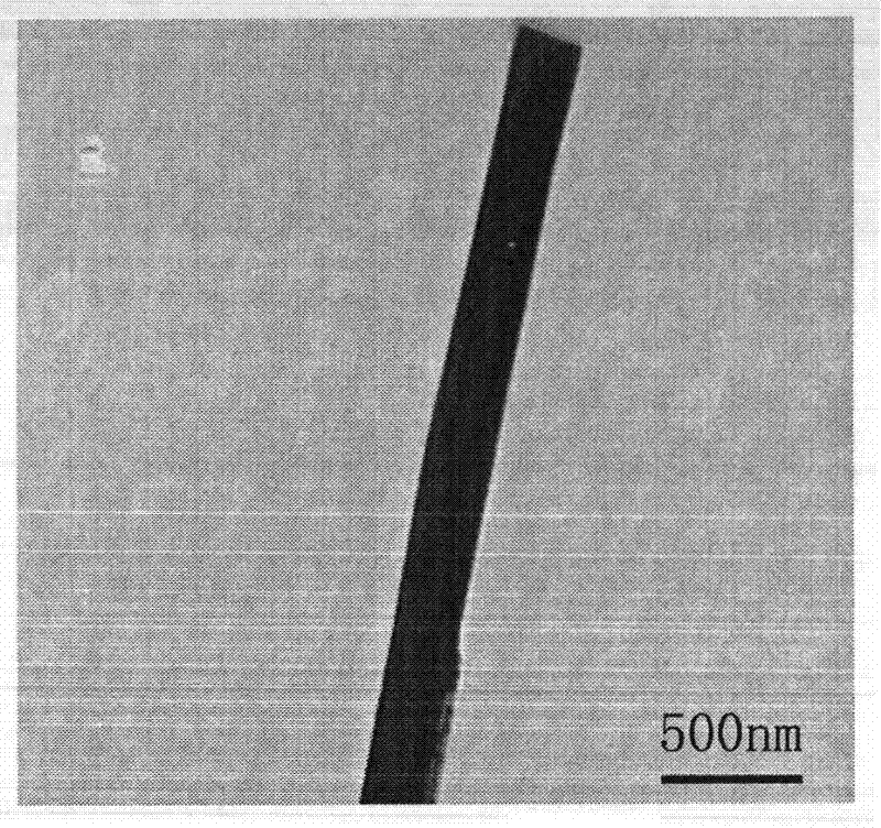
[0021] The first step is to use CdS powder as the raw material and Bi powder as the catalyst. After the two are uniformly mixed at 1mol:0.05mol, the powder is placed on the molybdenum heater, and the conductive surface of the ITO glass is used as the substrate. Place it at about 1.0cm above the evaporation source, airtight the evaporation chamber, when the vacuum degree is 1×10 -2 After Pa, the current was gradually increased to 120A at a current increase rate of 10A / 3.5min and kept for 10 minutes. A large area of ​​uniform yellow deposit is deposited on the surface of the substrate. Analyze and test this product and get: (1) by figure 1 XRD analysis showed that the product obtained was hexagonal CdS, which corresponds to card No. 65-3414 in the ICDD PDF card library; (2) SEM analysis showed that the product obtained was a large area, uniform nanowire. The diameter range is 80-300nm and the length is about 15-40μm (see figure 2 ); (3) by image 3 From the TEM image, it can be ...

Embodiment 2

[0023] The first step is to use CdS powder as the raw material and Bi powder as the catalyst. After the two are uniformly mixed at 1mol:0.05mol, the powder is placed on the molybdenum heater, and the conductive surface of the ITO glass is used as the substrate. Place about 1.0cm above the evaporation source, airtight the evaporation chamber, when the vacuum degree is 5×10 -2 After Pa, the current was gradually increased to 120A at a current increase rate of 10A / 3min and kept for 7min. A large area of ​​uniform yellow deposit is deposited on the surface of the substrate. In the second step, after taking out the sample, place it on a molybdenum heating boat using ZnS as a raw material, and use a large area of ​​uniformly grown CdS single crystal nanowire as a substrate, and place the substrate about 1.6 cm above the evaporation source, and seal it. Evaporation chamber, the vacuum degree is 1.7×10 -2 After Pa, the current was gradually increased to 140A at a current increase rate ...

Embodiment 3

[0025] The first step is to use CdS powder as the raw material and Bi powder as the catalyst. After the two are uniformly mixed at 1mol:0.05mol, the powder is placed on the molybdenum heater, the Si wafer is used as the substrate, and the substrate is placed in the evaporation source. At about 1.3cm above, the evaporation chamber is sealed, when the vacuum degree is 2×10 -2 After Pa, the current was gradually increased to 100A at a current increase rate of 10A / 3.5min and kept for 10 minutes. A large area of ​​uniform yellow deposit is deposited on the surface of the substrate. In the second step, after taking out the sample, place it on a molybdenum heater using ZnS as a raw material, and use a large area of ​​uniformly grown CdS single crystal nanowire as a substrate, and place the substrate about 1 cm above the evaporation source, and evaporate in a sealed manner. Chamber, the vacuum degree is 5×10 -2 After Pa, the current was gradually increased to 120A at a current increase...


PUM

PropertyMeasurementUnit
diameteraaaaaaaaaa
lengthaaaaaaaaaa

Abstract

The invention belongs to the field of nanowire heterojunction preparation, and relates to a method for growing CdS nanowires by a vacuum thermal evaporation method with the assistance of a catalyst and coating ZnS in its radial direction. The specific implementation process is as follows: first step, uniformly mix CdS and Bi powder at a ratio of 1:0.05mol as raw materials, place them in a resistance heating boat made of molybdenum sheets, and place a substrate at 1.0cm-2.0cm above the boat. During the evaporation process, the vacuum degree in the evaporation furnace is kept at 5×10⁻³Pa-5×10⁻²Pa, the heating current is 100A-120A, and the deposition time is 2min-10min to prepare CdS nanowires. In the second step, ZnS powder is used as a raw material, placed in a boat, and CdS nanowires are used as a substrate. Place the substrate at 1.0cm-2.0cm above the boat. During the evaporation process, the vacuum degree in the evaporation furnace is kept at 5×10⁻³Pa-5×10⁻²Pa, the deposition current is 120A-140A, and the deposition time is 2min-10min. Coating ZnS on CdS nanowires. Finally, CdS/ZnS nanowire radial heterojunction is obtained. The CdS/ZnS nanowire heterojunction obtained by the invention has the characteristics of good optical properties, uniform appearance, etc.; and the method is simple, easy to popularize, and suitable for large-scale industrial production.

Description

Technical field [0001] The invention belongs to the field of nano-heterojunction preparation, and is a method for growing CdS single crystal nanowires by vacuum thermal evaporation with the assistance of a catalyst, and then coating a ZnS polycrystalline layer in the radial direction, thereby obtaining a nanowire heterojunction . Background technique [0002] Semiconductor heterojunction is the basic unit in various optoelectronic devices, and has a wide range of important applications. Traditional semiconductor heterojunctions are generally realized in bulk or thin-film materials, with three-dimensional or two-dimensional properties in dimensions, and the scale is generally on the order of micrometers or more. [0003] In recent years, nano-science and technology have developed rapidly, and advanced devices with nano-materials as structural units have appeared and have shown some excellent properties. Studies have shown that as the size and latitude decrease, nanomaterials exhib...

Claims


Application Information

Patent Timeline
Patent Type & Authority Applications(China)
IPC IPC(8): H01L21/363B82Y40/00C23C14/26C23C14/06
Inventor 姚菊枚王贺勇杨冰杨林钰简基康
Owner XINJIANG UNIVERSITY
Why Eureka
Try Eureka