Semiconductor laser and light field splicing method for realizing large-angle uniform irradiation

A uniform irradiation and laser technology, applied in the field of lasers, to achieve the effects of narrow spectral width, uniform radiation, and high radiation power

Active Publication Date: 2011-11-30
THE 13TH RES INST OF CHINA ELECTRONICS TECH GRP CORP
View PDF5 Cites 9 Cited by
  • Summary
  • Abstract
  • Description
  • Claims
  • Application Information

AI Technical Summary

Problems solved by technology

Therefore, in the case of limited light source volume, it is impossible to achieve unifor...

Method used


Image

  • Semiconductor laser and light field splicing method for realizing large-angle uniform irradiation
  • Semiconductor laser and light field splicing method for realizing large-angle uniform irradiation
  • Semiconductor laser and light field splicing method for realizing large-angle uniform irradiation

Examples


Embodiment 1

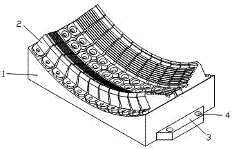
[0033] Embodiment 1 (the embodiment of semiconductor laser described in the present invention, see Figure 1-Figure 3 ):

[0034] A semiconductor laser that realizes large-angle uniform irradiation is characterized in that it includes a base 1 whose upper surface is an arc surface and at least one set of laser array unit groups arranged in the direction of the fast axis; the laser array unit group consists of at least one in the slow The laser array unit 2 arranged in the axial direction is composed of; the number of the laser array unit group is the required angle of irradiation of the laser in the fast axis direction / the full width at half maximum angle of the slow axis of the bar 21; the number of laser array units 2 in the laser array unit group : The laser irradiates the required angle in the direction of the slow axis / the angle at half maximum of the slow axis of the bar 21;

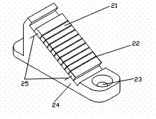
[0035] The laser array unit includes a triangular wedge-shaped tube base 24, a semiconductor l...

Embodiment 2

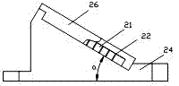
[0043] Embodiment 2 (the embodiment of the element splicing method of the semiconductor laser described in the present invention, see figure 1 —3):

[0044]Realize the method for splicing the light field of the semiconductor laser of large-angle uniform irradiation, it is characterized in that carrying out according to the following steps:

[0045] 1) Calculate the number of laser array unit groups: the required angle of irradiation of the laser in the direction of the fast axis / the angle of the full width at half maximum of the slow axis of the laser;

[0046] 2) Determine the angle α of the triangular wedge-shaped tube seat: it is the complementary angle of the fast axis full width at half maximum angle of the laser;

[0047] 3) Calculate the number of bars 21 included in the semiconductor laser core group: total output power required by the laser / output power of each bar;

[0048] 4) Calculate the number of laser array units 2 in the laser array unit group: the required a...


PUM

PropertyMeasurementUnit
Luminous poweraaaaaaaaaa

Abstract

The invention discloses a semiconductor laser capable of realizing wide-angle uniform shining and a light field splicing method. The semiconductor laser comprises a base the upper surface of which is an arc surface and at least one set of laser array unit sets, wherein each laser array unit set comprises at least one laser array unit; each array unit comprises a triangular wedge-shaped tube seat,a semiconductor laser core set, two electrode leads and a quartz scattering piece, wherein the semiconductor laser core set is located on the upper surface of the tube seat, the two electrode leads are led out from the two ends of each semiconductor laser core set, and the quartz scattering piece covers on the semiconductor laser core set. The invention has the advantages that the asymmetric character of the light fields of the semiconductor laser in two directions is fully utilized, diffident quantities of laser arrays are respectively used for splicing in the slow axis and fast axis directions of the laser in accordance with a specific curve support and a unit array with a specific angle so as to realize equivalent diffusion angle, uniform-radiation wide angle and high-power light source irradiation in the slow axis and fast axis directions.

Description

technical field [0001] The invention relates to a laser, in particular to a semiconductor laser for realizing large-angle uniform irradiation and a unit splicing method. Background technique [0002] In recent years, laser illumination imaging technology has developed rapidly, especially active laser illumination imaging technology has achieved considerable development in the industrial and military fields. [0003] The principle of active laser illumination imaging technology is basically the same as that of lidar. Near-infrared lasers are used as illumination sources to detect and image long-distance targets under low illumination conditions. According to the different light emitting forms of the illumination source, the active laser illumination imaging system can be divided into continuous laser illumination imaging system and pulse illumination imaging system. The continuous laser illumination imaging system uses continuous semiconductor lasers to illuminate the target...

Claims


Application Information

Patent Timeline
IPC IPC(8): H01S5/40H01S5/024
Inventor 王晓燕闫立华赵润常会增徐会武陈宏泰安振峰
Owner THE 13TH RES INST OF CHINA ELECTRONICS TECH GRP CORP
Why Eureka
Try Eureka