Wafer level packaging structure and packaging method

A wafer-level packaging and wafer technology, which is applied in the manufacturing of electrical components, electrical solid-state devices, semiconductor/solid-state devices, etc., can solve problems such as poor product reliability, wafer-level packaging open circuit, etc. High consistency and good thickness uniformity

Inactive Publication Date: 2011-12-07
CHINA WAFER LEVEL CSP
View PDF5 Cites 10 Cited by
  • Summary
  • Abstract
  • Description
  • Claims
  • Application Information

AI Technical Summary

Problems solved by technology

[0009] However, the wafer-level packaging formed by the above process may hav

Method used


Image

  • Wafer level packaging structure and packaging method
  • Wafer level packaging structure and packaging method
  • Wafer level packaging structure and packaging method

Examples


Embodiment Construction

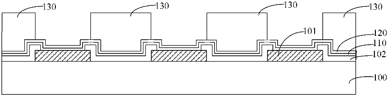
[0031] After a lot of experiments, the inventors of the present invention found that the open circuit phenomenon in the wafer-level packaging of the existing technology is caused by the following reasons: the distance between the chip pads is getting narrower, and the copper metal pillar 131 has a certain Height, so that the opening of the photoresist pattern is small, the aspect ratio of the copper metal column 131 to be formed is large, and bubbles are prone to appear during the electroplating process, resulting in an open circuit in the subsequent packaging process; and the inventor of the present invention also in the experiment It is found that the lower reliability of products packaged by the existing wafer-level packaging process is due to: the electroplating process is used in the existing packaging process, and the surface of the copper metal pillar 131 after electroplating is not flat, so that the solder layer 132 is not in contact with the non-flat surface. The flat ...


PUM


Abstract

A wafer-level packaging structure and packaging method, wherein the wafer-level packaging method includes: providing a wafer to be packaged, a plurality of discrete pads are formed on the surface of the wafer; forming conductive contour columns on the surface of the pads ; Form bumps on the surface of the contour column. The wafer-level packaging method provided by the invention has a simple process, and the wafer-level packaging structure provided by the invention has high packaging quality.

Description

technical field [0001] The invention relates to the field of chip packaging, in particular to a wafer-level packaging structure and packaging method. Background technique [0002] As the size of the chip becomes smaller and the function becomes stronger, the number of pads increases and the spacing becomes narrower. Correspondingly, higher requirements are put forward for the chip package. [0003] The traditional chip packaging method usually uses wire bonding (Wire Bonding) for packaging, but with the rapid development of chips, wafer-level packaging gradually replaces wire bonding. In the Chinese patent document with the publication number CN101740422A, it can be found that more More information about wafer level packaging. [0004] The existing wafer-level packaging process specifically includes: Please refer to figure 1 , providing a wafer 100 to be packaged, the surface of the wafer 100 to be packaged has a plurality of discrete pads 101 and a passivation layer 102, ...

Claims


Application Information

Patent Timeline
IPC IPC(8): H01L21/60H01L23/498
CPCH01L24/11H01L2224/1403H01L2224/11H01L2924/00012
Inventor 王宥军俞国庆杨红颖王蔚
Owner CHINA WAFER LEVEL CSP
Why Eureka
Try Eureka