A multi-source integrated color-tunable light-emitting element and its preparation method

A technology for light-emitting components and colors, applied in electrical components, semiconductor devices, circuits, etc., can solve the problems of difficult wavelength control, difficult light color mixing to achieve ideal effects, and high control requirements for quantum dot growth.

Inactive Publication Date: 2011-12-07
楼刚
View PDF5 Cites 17 Cited by
  • Summary
  • Abstract
  • Description
  • Claims
  • Application Information

AI Technical Summary

Problems solved by technology

A display screen requires a large number of LED particles, but the color difference of LEDs in different production batches is large, and due to the size limitation of LED particles, the resolution at close range is low, resulting in the narrowing of the application range of LED display screens
Although the method of externally coating phosphor powder is low in cost and simple in process, the phosphor powder is prone to failure, resulting in a reduction in the life of the entire LED, and the luminous efficiency of the phosphor powder limits the overall luminous efficiency of the LED.
[0003] A published patent (application number CN200410009267.3, quantum dot active region structure and epitaxial growth method of wide-spectrum white light LED) proposes a method of using quantum dots to manufacture white light LEDs, which uses self-organized growth methods to grow quantum dots, The size of quantum dots fluctuates randomly and the spectrum is wide, but the control requirements for quantum dot growth are high, the wavelength is easy to shift, and the purity of color cannot be controlled
A published patent (application number CN 200410000148.1, light-emitting diode structure) proposes to use quantum wells with different wavelengths to be stacked in the active layer to emit red, green, and blue light at the same time to manufacture white LEDs. However, different quantum wells interfere with each other, and the wavelength is affected by the current and voltage. The influence is difficult to control, and the color mixing of light is difficult to achieve the desired effect

Method used


Image

  • A multi-source integrated color-tunable light-emitting element and its preparation method
  • A multi-source integrated color-tunable light-emitting element and its preparation method
  • A multi-source integrated color-tunable light-emitting element and its preparation method

Examples


Embodiment 1

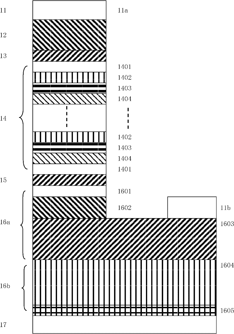
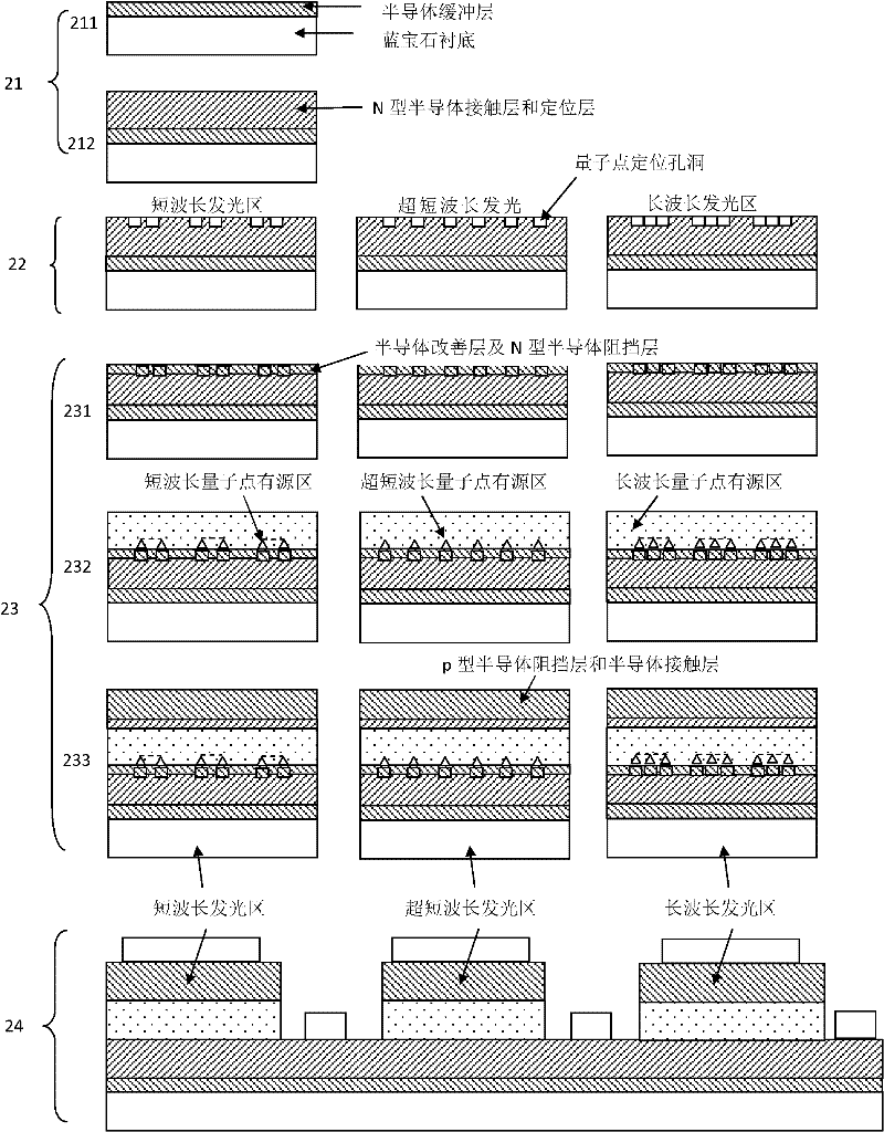
[0070] Red, green and blue three-color integrated tunable gallium nitride (GaN)-based light-emitting element, the schematic diagram of the single-wavelength light-emitting part thereof is shown in figure 1 , bottom-up including:

[0071] (1) Substrate 17

[0072] A transparent growth substrate 17, the material of which can be sapphire;

[0073] (2) Buffer layer 16b

[0074] The side close to the substrate 17 is a layer of about 1000nm GaN buffer layer 16b, which can be n-doped or undoped according to the chip structure. The buffer layer in this embodiment at least includes a 15-25nm GaN nucleation layer 1605 and a 1μm GaN layer 1604 for reducing lattice mismatch;

[0075] (3) n-type semiconductor contact layer 16a

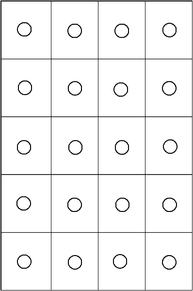
[0076] Above the buffer layer 16b is an n-type semiconductor contact layer 16a of about 2000nm GaN material, which includes: a 500nm n-type GaN positioning layer 1602, this embodiment uses 500nm GaN:Si, n≥5×10 18 cm -3 , used to etch into a quantum dot positi...

Embodiment 2

[0119] Red, green and blue three-color integrated tunable gallium nitride (GaN)-based light-emitting element, the schematic diagram of the single-wavelength light-emitting part thereof is shown in Figure 5 , bottom-up including:

[0120] (1) substrate 57;

[0121] (2) buffer layer 56b;

[0122] (3) n-type semiconductor contact layer 56a;

[0123] (4) n-type semiconductor barrier layer 55;

[0124] (5) Active layer 54;

[0125] (6) p-type semiconductor barrier layer 53;

[0126] (7) p-type semiconductor contact layer 52;

[0127] (8) Electrode layer 51 .

[0128] The difference between the single emission wavelength structure of this embodiment and Embodiment 1 lies in the active layer. Its active layer 54 uses mixed quantum dots and quantum wells as the main light-emitting structure, and from bottom to top at least includes:

[0129] 5-20nm GaN underlying semiconductor pad layer 5401; its energy gap is larger than that of the quantum dot layer 5407, but smaller than or ...


PUM


Abstract

The invention relates to a multi-source integrated color-adjustable light-emitting component and a preparation method thereof. The multi-source integrated color-adjustable light-emitting component and preparation method have the advantages of effectively prolonging the service life of products and increasing the light conversion efficiency of light emitting diodes. The multi-source integrated color-adjustable light-emitting component comprises an electrode layer, a p-type semiconductor contact layer, a p-type semiconductor barrier layer, an active layer, an n-type semiconductor barrier layer,an n-type semiconductor contact layer, and a substrate, which are arranged in sequence from top to bottom, wherein the electrode layer is formed by a plurality of p electrodes and a plurality of n electrodes, which are spaced according to different light wavelength regions, and at least one type of electrodes are insulated from one another to independently regulate and control the regions of different light wavelengths; the energy gap of the p-type semiconductor barrier layer is wider than that of the p-type semiconductor contact layer; the light wavelength range of the active layer is from red light to blue light, the active layer has a light-emitting structure formed by quantum dots and quantum wells, and the positions of the quantum dots are restricted in corresponding regions; and theenergy gap of the n-type semiconductor barrier layer is wider than that of the n-type semiconductor contact layer.

Description

technical field [0001] The invention relates to a light-emitting element, in particular to a multi-source integrated color-adjustable light-emitting element and a preparation method thereof, belonging to the technical field of optoelectronic devices. Background technique [0002] As a solid-state light source, LED has many advantages such as small size, long life, high brightness, low energy consumption, no secondary pollution, and easy integration. As a green lighting source, it has gradually entered general lighting from the field of high-end lighting. Monochromatic LEDs have been commercialized, but because of their single color, white light must be emitted through a combination of multiple LEDs, such as the three-primary color method and the blue-yellow light mixing method, or the externally coated phosphor stimulated emission of other color light methods. The combination method of multiple LEDs has flexible luminous colors, but it is difficult to mass-produce, and it is...

Claims


Application Information

Patent Timeline
Patent Type & Authority Applications(China)
IPC IPC(8): H01L33/06H01L33/00
Inventor 楼刚兰红波
Owner 楼刚
Why Eureka
Try Eureka