A positive high voltage level conversion circuit

A technology of voltage conversion circuit and conversion circuit, which is applied in the direction of logic circuit connection/interface layout, logic circuit coupling/interface using field effect transistors, etc., which can solve the problems of increasing process cost, increasing NMOS transistors, and reducing conduction capacity. , to achieve the effect of enhanced driving capability, simple circuit structure and fast switching speed

Inactive Publication Date: 2011-12-07
TSINGHUA UNIV
View PDF4 Cites 24 Cited by
  • Summary
  • Abstract
  • Description
  • Claims
  • Application Information

AI Technical Summary

Problems solved by technology

[0009] However, for figure 2 In the traditional positive high-voltage level switching circuit shown, when the VDD power supply voltage drops, the gate drive voltages of the NMOS transistor 202 and the NMOS transistor 204 drop, so their conduction capabilities will drop, resulting in the difference between the PMOS transistor and the NMOS transistor during the level shifting process. Increased competition among transistors, large level transition delays and transition power consumption
When the VDD power supply voltage drops further, there may even be a problem that the circuit cannot switch the high voltage normally
The method of simply increasing the size of the NMOS transistor will lead to a sharp increase in the area of ​​the switching circuit, which increases the process cost
In addition, due to the large number of word lines and bit lines in the flash memory system, the performance degradation of the high-voltage switching circuit will seriously affect the performance of the entire flash memory system

Method used


Image

  • A positive high voltage level conversion circuit
  • A positive high voltage level conversion circuit
  • A positive high voltage level conversion circuit

Examples


Embodiment Construction

[0019] The present invention will be further described below in conjunction with the accompanying drawings.

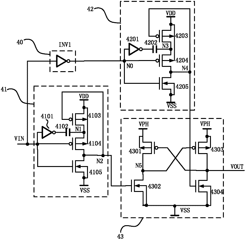
[0020] Such as image 3 As shown, the connection relationship of a positive high-voltage level conversion circuit is as follows: the VIN input voltage is connected to the common node of the INV1 inverter 40 and the first bootstrap circuit 41, and the INV1 inverter 40 is also connected to the second bootstrap circuit 42 , the voltage converting circuit 43 is respectively connected to the first bootstrap circuit 41, the second bootstrap circuit 42 and the VOUT output voltage.

[0021] The connection relationship of the first bootstrap circuit 41 is as follows: the VIN input voltage is respectively connected to the input terminal of the first inverter 4101, the gate of the second PMOS transistor 4104 and the gate of the first NMOS transistor 4105, and the first inverter 4101 It is connected in series with the first capacitor 4102, the N1 node is respectively connected to...


PUM


Abstract

The invention discloses a positive high voltage level conversion circuit, which belongs to the technical field of integrated circuit designing. Connection relationships of parts of the positive high voltage level conversion circuit are that: an input voltage VIN is connected with a common node of an inverter INV1 and a first bootstrap circuit; the inverter INV1 is also connected with a second bootstrap circuit; and a voltage conversion circuit is connected with the first bootstrap circuit, the second bootstrap circuit and an output voltage VOUT. The positive high voltage level conversion circuit has the advantages that: the circuit has a simple circuit structure, high conversion speed and low power consumption; the two bootstrap circuits increases the amplitude of oscillator of a low voltage control signal once and enhances the driving capability of two high voltage N-channel metal oxide semiconductor (NMOS) transistors in the voltage conversion circuit, thereby reducing stiff competition between a pull-down NMOS transistor and a pull-up P-channel metal oxide semiconductor (PMOS) transistor in a voltage conversion process of the voltage conversion circuit and reducing the power consumption for high voltage conversion; and the circuit still can work normally under low power voltage.

Description

technical field [0001] The invention belongs to the technical field of integrated circuit design, and in particular relates to a positive high-voltage level conversion circuit. Background technique [0002] At present, flash memory (Flash memory) is widely used in portable devices such as mobile phones, cameras, and handheld computers. It has the advantages of not losing data when power is turned off, high programming speed, and high integration. figure 1 is a cross-sectional view of a traditional flash memory unit, which is a stacked gate structure composed of a polysilicon control gate 10 and a floating gate 12 . On the p-type substrate 16, a source 14 and a drain 15 of n+ structure are formed by implantation. In addition, the floating gate 12 is isolated from the p-type substrate 16 by the second insulating layer 13 , and the polysilicon control gate 10 is isolated from the floating gate 12 by the first insulating layer 11 . This stacked gate structure makes the thresho...

Claims


Application Information

Patent Timeline
Patent Type & Authority Applications(China)
IPC IPC(8): H03K19/0185
Inventor 王雪强刘培军潘立阳伍冬周润德
Owner TSINGHUA UNIV
Why Eureka
Try Eureka