
Method and device for optically measuring product surfaces

An optical and product technology, applied in the direction of using optical devices, measuring devices, instruments, etc., can solve the problems of scanning speed limitation, not allowing access to surface height information, maximum scanning width limitation, etc., to increase measurement accuracy and reduce shadows and lighting effects, the effect of increasing the scan width

Active Publication Date: 2011-12-14
WITRINS S R O
View PDF2 Cites 23 Cited by
  • Summary
  • Abstract
  • Description
  • Claims
  • Application Information

AI Technical Summary

Problems solved by technology

[0004] Known methods according to the prior art do not allow obtaining surface height information with an accuracy of less than + / - 20 μm
Additionally, the maximum scan width of the product being measured is limited, making it infeasible to scan products wider than 150mm
Scanning speed is limited, thus making surface measurement a bottleneck for high-speed production processes

Method used


Image

  • Method and device for optically measuring product surfaces
  • Method and device for optically measuring product surfaces
  • Method and device for optically measuring product surfaces

Examples


Embodiment approach 15

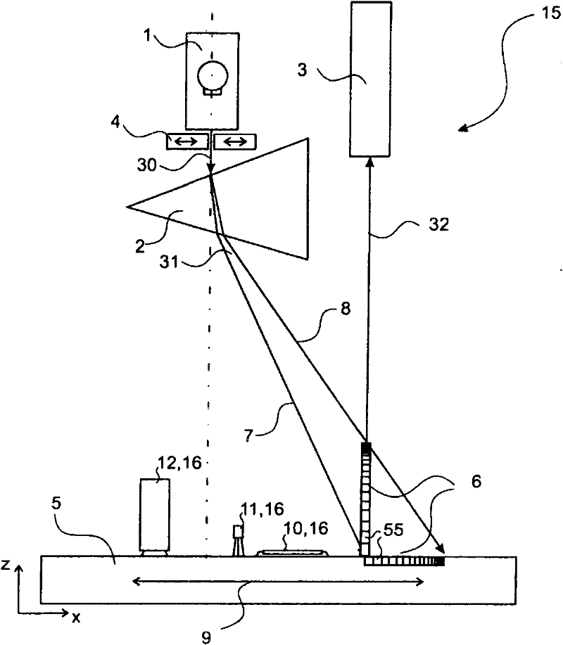
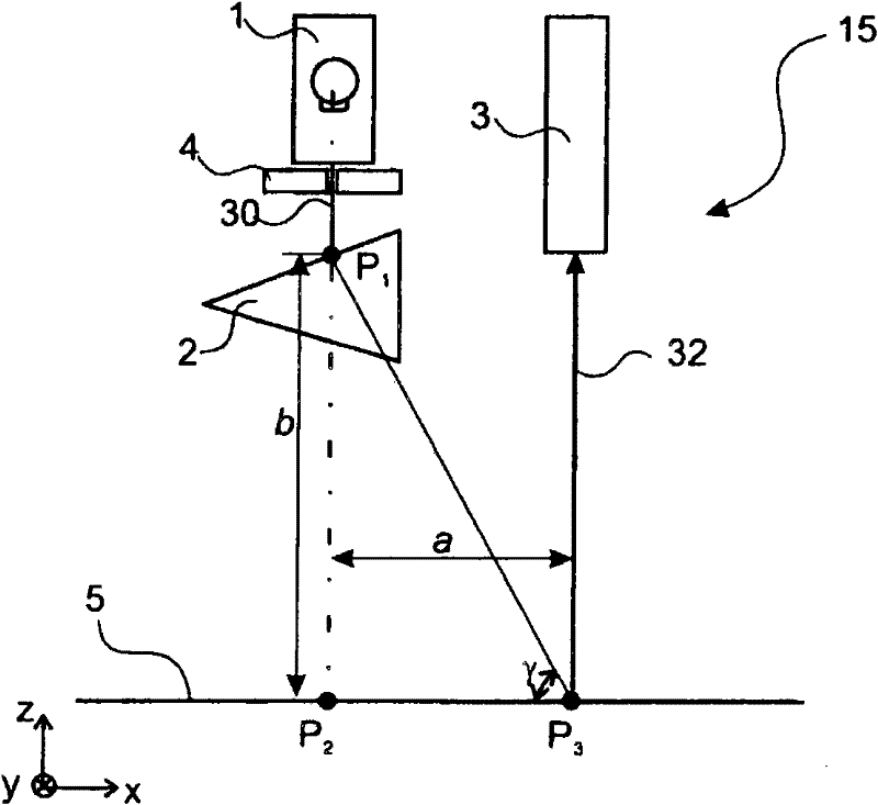
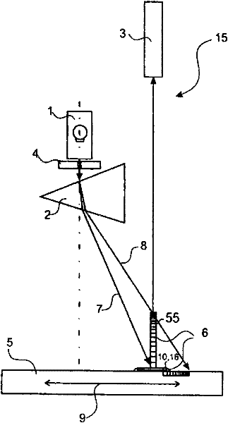
[0072] A first embodiment 15 for measuring a product under test in order to optically create a 3D model is shown in FIG. 1 and comprises a white light source 1 with white light of a continuous spectrum, for rectifying the white light and Optical unit 4 for collimation into collimated white light beam 30 , optical prism 2 for splitting collimated white light beam 30 into polychromatic beam 31 and RGB line scan camera 3 . The light from the source 1 is collimated by the optical unit 4 into parallel narrow beams 30 which then pass through the optical prism 2 which acts as a spectrometer unit and intermediaries to facilitate the splitting of the light into spectra 13( Figure 5 ). The collimated light 30 entering the prism 2 contains all color elements. After passing through the optical prism 2, the white light 30 is resolved into individual colors 31 according to the laws of refraction of light. These individual components are monochromatic and are reflected via monochromatic l...


PUM


Abstract

The present invention relates to a device (10), a method and an application thereof for optically measuring the surface of a tested product (5), especially a PCB-product for reflow soldering paste inspection. The device comprises at least one white light source (1) for emitting a beam of white light, at least one collimation unit (4) for collimating said beam of white light (30), at least one spectrometer unit, preferably an optical prism (2) or an optical diffraction grading (51), for splitting said beam of white light (30) into a beam of multichromatic light (31) being directed onto said tested product (5) under a predetermined incident angle γ, and at least one camera (3) for recording a reflected beam of monochromatic light (32) of said tested product (5). Z-axis surface height information of said tested product (5) can be extracted from a hue value of said reflected beam of mono chromatic light (32) while relatively moving said tested product (5) in a x-axis scanning direction (9).

Description

technical field [0001] The present invention generally relates to apparatus and methods for measuring and checking the distance between a sensor and a product under test. In particular, the present invention can be used in the field of electronics for measuring and testing the position of components mounted on printed circuit boards (PCBs) or solar cell products, or for reflowing electronic components mounted on PCBs Check the position of connectors of electronic components such as ICs, capacitors, transistors, resistors, etc., or the position of reflowed solder paste before soldering. The invention is preferably applicable to the production of PCBs, solar cell products such as solar cell wafers or solar cell components, and other items where flatness needs to be measured in order to thus specify its quality, and can also be used to test product surfaces surface roughness. The present invention can also be used to inspect the three-dimensional shape of various items while re...

Claims


Application Information

Patent Timeline
Patent Type & Authority Applications(China)
IPC IPC(8): G01B11/06G01B11/25
CPCG01B2210/50G01B11/0608G01B11/2509H05K13/0817
Inventor R·F·维泽
Owner WITRINS S R O
Learn More