A kind of sintering mold of thyristor chip and molybdenum sheet and using method thereof

A technology of silicon chips and molds, applied in electrical components, semiconductor/solid-state device manufacturing, circuits, etc., can solve the dislocation of silicon chips and molybdenum chips, the influence of product flow capacity and appearance, and the sintering process of molybdenum chips and silicon chips Not too standardized and other issues, to achieve the effect of improving production efficiency and good heat transfer

Active Publication Date: 2011-12-21
捷捷半导体有限公司
View PDF4 Cites 7 Cited by
  • Summary
  • Abstract
  • Description
  • Claims
  • Application Information

AI Technical Summary

Problems solved by technology

[0003] At present, modules of power semiconductor devices (including modules and solid-state relays) are widely used, and there are many manufacturers, but most of the sintering processes of molybdenum chips and silicon chips are not standardized, especially for the positioning of silicon chips and molybdenum chips. They are relatively rough, often causing dislocation of silicon chips and molybdenum chips, which affects the flow capacity and appearance of the product to varying degrees.

Method used


Image

  • A kind of sintering mold of thyristor chip and molybdenum sheet and using method thereof
  • A kind of sintering mold of thyristor chip and molybdenum sheet and using method thereof
  • A kind of sintering mold of thyristor chip and molybdenum sheet and using method thereof

Examples


Embodiment Construction

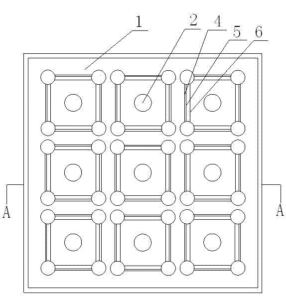
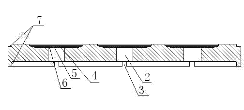
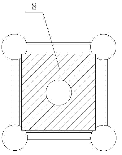
[0028] Such as figure 1 and 2 As shown, a sintering mold of a thyristor chip and a molybdenum sheet of the present invention comprises a sintering mold body 1, and a plurality of holes 2 that are convenient for vertical exhaust are arranged in the middle of the sintering mold body 1, so as to facilitate vertical exhaust. Below the hole 2, there is a hole 3 for horizontal exhaust, and the top of the hole 2 for vertical exhaust is provided with an upper positioning step 4, a middle positioning step 5 and a lower positioning step 6 from top to bottom, and the sintering mold body 1 is surrounded. There are steps 7 for stacking, the diameter of the lower positioning step 6

[0029] The mold material adopts electronic graphite, which can ensure good heat transfer during the sintering process and can make the three-layer parts of the product be positioned reliably; the thermal conductivity is...


PUM


Abstract

The invention relates to a sintering mold for controlled silicon chips and molybdenum pieces. The sintering mold comprises a sintering mold body. A plurality of parts are arranged on the sintering mold body. The center of each part is provided with a hole convenient for longitudinal exhausting. Holes convenient for transverse exhausting are formed below the holes convenient for the longitudinal exhausting. The top of the hole convenient for the longitudinal exhausting is provided with an upper-layer positioning step, a middle-layer positioning step and a lower-layer positioning step sequentially from top down. The periphery of the sintering mold body is provided with steps. The invention also relates to a using method of the sintering mold for the controlled silicon chips and the molybdenum pieces. The using method comprises the following steps of: 1, arranging cathode molybdenum pieces with silver-plated surfaces into the lower-layer positioning steps of the mold; 2, dispensing soldering paste on the cathode molybdenum pieces by using a corresponding adhesive dispensing head; 3, arranging the controlled silicon chips into the middle-layer positioning steps of the mold; 4, dispensing the soldering paste on the chips by using the corresponding adhesive dispensing head; and 5, arranging anode molybdenum pieces with silver-plated surfaces into the upper-layer positioning steps ofthe mold. The sintering mold and the using method have the advantages that: positioning accuracy and high heat-conducting properties are ensured; the mold has high permeability; and convenience is brought to vacuum extraction and the removal of soldering flux from the soldering paste.

Description

technical field [0001] The invention relates to a sintering mold for a thyristor chip and a molybdenum sheet, and belongs to the technical field of packaging of semiconductor devices. [0002] The invention also relates to a method for using a sintering mold of a thyristor chip and a molybdenum sheet. Background technique [0003] At present, modules of power semiconductor devices (including modules and solid-state relays) are widely used, and there are many manufacturers, but most of the sintering processes of molybdenum chips and silicon chips are not standardized, especially for the positioning of silicon chips and molybdenum chips. They are relatively rough, often resulting in the dislocation of silicon chips and molybdenum chips, which affects the flow capacity and appearance of the product to varying degrees. Therefore, it is necessary to provide a new technical solution to solve the above technical problems. Contents of the invention [0004] The object of the pre...

Claims


Application Information

Patent Timeline
Patent Type & Authority Applications(China)
IPC IPC(8): H01L21/50
Inventor 王琳吴家健
Owner 捷捷半导体有限公司
Why Eureka
Try Eureka