A charge pump circuit and flash memory using the charge pump circuit

A flash memory and charge pump technology, applied in static memory, read-only memory, information storage, etc., can solve the problems of low current drive capability of charge pump, large chip area, and improved integration, so as to improve current drive capability , Improve chip integration, reduce the effect of area

Active Publication Date: 2011-12-21
SHANGHAI HUAHONG GRACE SEMICON MFG CORP
View PDF4 Cites 20 Cited by
  • Summary
  • Abstract
  • Description
  • Claims
  • Application Information

AI Technical Summary

Problems solved by technology

[0006] The problem solved by the present invention is to provide a charge pump circuit and a flash memory using the charge pump circuit, to solve the problem that the output capacitor in the existing charge pump circuit occupies a large chip area, which is not conducive to improving the integration degree, and the charge The problem that the current drive capability of the pump is not high

Method used


Image

  • A charge pump circuit and flash memory using the charge pump circuit
  • A charge pump circuit and flash memory using the charge pump circuit
  • A charge pump circuit and flash memory using the charge pump circuit

Examples


Embodiment Construction

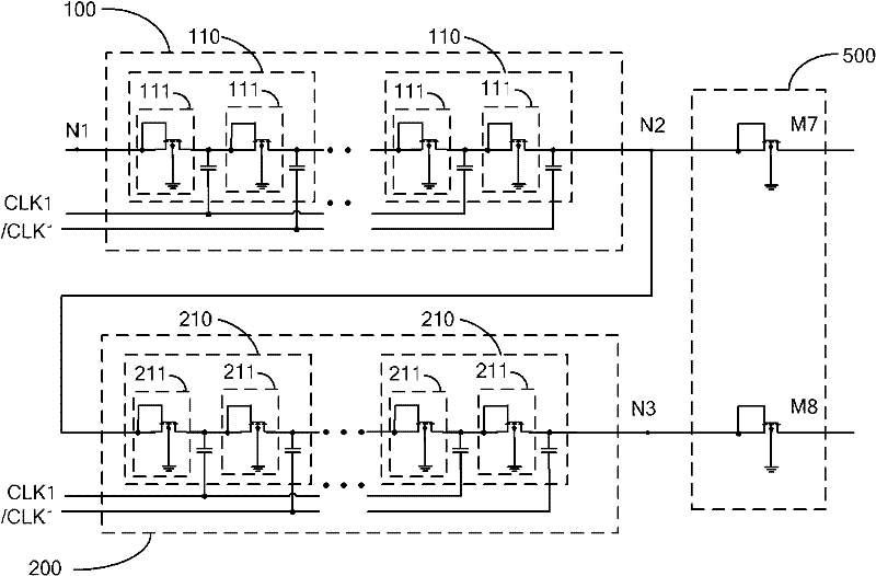
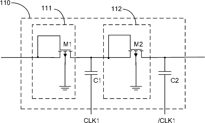
[0032] In order to make the above objects, features and advantages of the present invention more comprehensible, specific implementations of the present invention will be described in detail below in conjunction with the accompanying drawings.

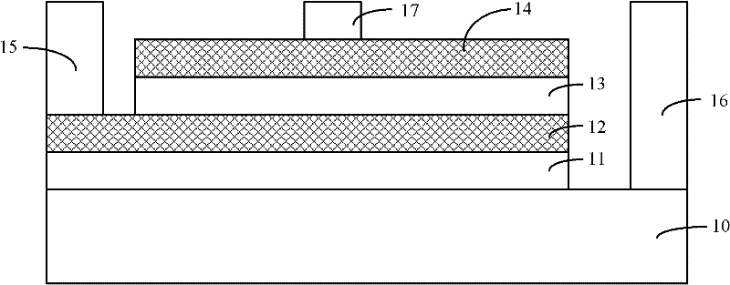
[0033] Since the output voltage is lower in the basic units at all levels before the charge pump is boosted to the voltage required for data programming, the charge stored in the output capacitor is less, and the use of a large-capacity MOS capacitor to store less charge will cause waste, and Large-capacity MOS capacitors occupy a large chip area, which is not conducive to improving chip integration.

[0034] And because the programming of flash memory data adopts hot electron injection, the output of the charge pump requires a large charge pump current drive capability, and a capacitor with a large capacitance per unit area is required; since the erasing of flash memory data uses a tunnel By way of effect, the charge pump output can r...


PUM


Abstract

A charge pump circuit, wherein a first charge pump unit, a second charge pump unit and an output unit are connected in series in sequence, the output ends of the first charge pump unit and the second charge pump unit are connected to the output unit, and the first charge pump The unit and the second charge pump unit are formed by cascading several basic units. The basic unit at least includes a switch unit and an output capacitor. An output capacitor is connected between two series-connected switch units. The first charge pump unit of the first charge pump unit The first output capacitor is a PPS capacitor, and the second output capacitor of the second charge pump unit is a MOS capacitor; the output unit is used to output the voltage output by the first charge pump unit and the voltage output by the second charge pump unit. Also provided is a flash memory using the charge pump circuit. Using the PPS capacitor as the output capacitor of the first charge pump unit can greatly reduce the area of ​​the output capacitor, improve chip integration, and improve the current driving capability of the first charge pump unit.

Description

technical field [0001] The present invention relates to a DC voltage step-up circuit, in particular to a charge pump circuit for boosting a DC voltage and a flash memory using the charge pump circuit. Background technique [0002] In integrated circuit systems, there are often many circuits that require DC voltages higher than the supply voltage for specific operations. For example, in flash memory, a higher voltage must be generated for data programming and erasing. The flash memory includes a plurality of memory cell arrays. Usually, each memory cell is a field effect transistor (FET), and the field effect transistor includes a floating gate located on the surface of the tunnel oxide layer. The floating gate can accumulate charges, so The charge corresponds to one bit of data information. The programming and erasing of memory data is carried out by controlling the injection and release of charges in the floating gate. The programming of memory data needs to inject the c...

Claims


Application Information

Patent Timeline
Patent Type & Authority Applications(China)
IPC IPC(8): H02M3/07G11C16/06
Inventor 王磊杨光军
Owner SHANGHAI HUAHONG GRACE SEMICON MFG CORP
Why Eureka
Try Eureka