Programmable Noise Threshold for Audio Amplifiers Using Low Noise and Noise Rejection Combined Analog and Digital Signal Processing
A noise threshold and amplifier circuit technology, applied in the field of volume control circuit architecture, can solve problems such as degraded analog circuit performance
- Summary
- Abstract
- Description
- Claims
- Application Information
AI Technical Summary
Problems solved by technology
Method used
Image
Examples
example 1
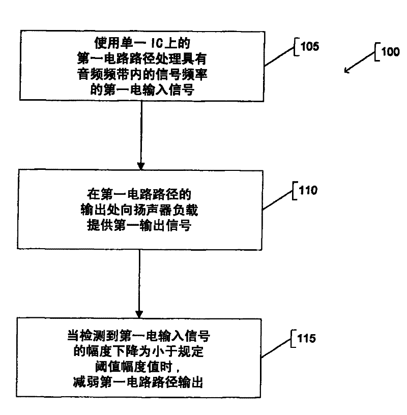
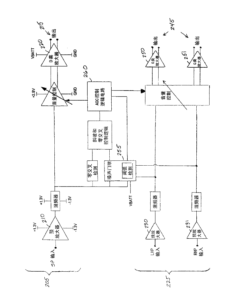
[0071] Example 1 includes subject matter (e.g., an apparatus formed on a single IC) comprising a first signal circuit path for processing a first electrical signal comprising one or more signal frequencies in the audio frequency band, wherein the first A signal circuit path includes: a first amplifier circuit configured to provide a first output signal to a speaker load; a noise threshold circuit configured to monitor the first electrical signal and generating a first indication when falling below a first specified threshold voltage value; and a control circuit coupled in phase with the noise gate circuit and the first signal circuit path, wherein the control circuit is configured to determine the The output of the first signal path is attenuated.
[0072] In Example 2, the subject matter of Example 1 optionally includes a second circuit path for processing a second electrical signal and a third electrical signal each having a frequency in the audio frequency band, wherein the...
example 3
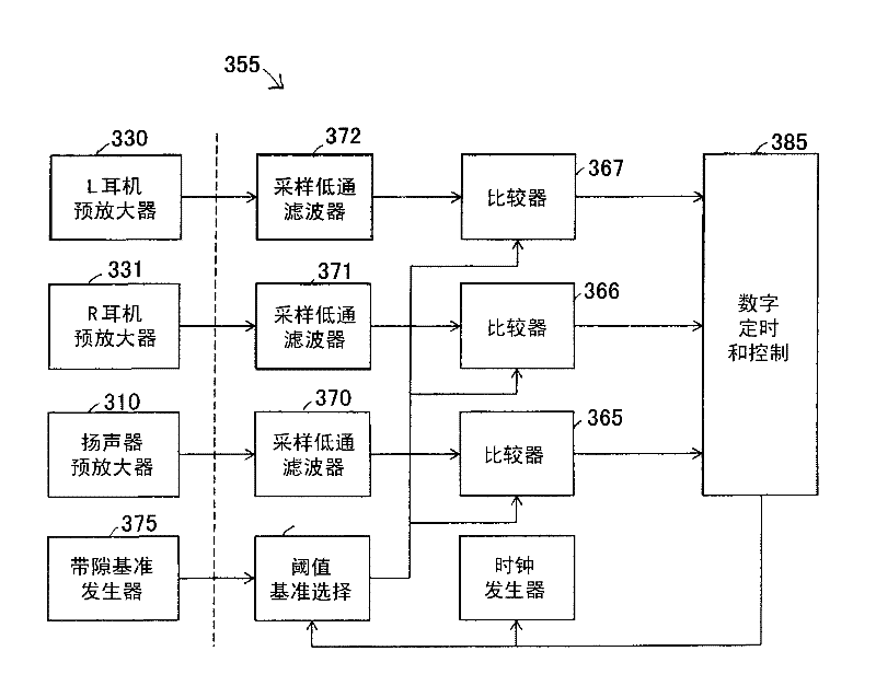
[0073] In Example 3, the first amplifier circuit of one or any combination of Examples 1 to 2 may optionally be a switching amplifier circuit configured to provide a first output signal to be connected between the circuit power supply and the IC ground switching between speaker loads, and the noise threshold circuit may optionally include: a charge pump circuit coupled in phase with the second and third amplifier circuits, wherein the charge pump is configured to generate The positive and negative power supply rails of the three-amplifier circuit; and a discrete-time low-pass filter circuit configured to filter the first electrical signal and at least one of the second and third electrical signals, wherein the discrete-time The sampling rate of the temporal filter reduces aliasing noise at zero hertz (0 Hz) due to switching of the switching amplifier and the charge pump circuit.
[0074] In Example 4, the switching frequency of the charge pump circuit of Example 3 may optional...
example 5
[0075] In Example 5, the output of the noise gate circuit of one or any combination of Examples 1 to 4 may optionally include a finite impulse response (FIR) low-pass filter to smooth the noise in the first and second indications. Generation of at least one.
PUM
 Abstract
Description
Claims
Application Information
 - R&D
- Intellectual Property
- Life Sciences
- Materials
- Tech Scout
- Unparalleled Data Quality
- Higher Quality Content
- 60% Fewer Hallucinations
Browse by: Latest US Patents, China's latest patents, Technical Efficacy Thesaurus, Application Domain, Technology Topic, Popular Technical Reports.
© 2025 PatSnap. All rights reserved.Legal|Privacy policy|Modern Slavery Act Transparency Statement|Sitemap|About US| Contact US: help@patsnap.com


