Electronic component embedded circuit board and manufacturing method thereof

A technology of electronic components and manufacturing methods, which is applied in the direction of assembling printed circuits with electrical components, printed circuit manufacturing, and printed circuits connecting non-printed electrical components, etc. Incompatibility of circuit board manufacturing process, corrosion and damage of aluminum electrode chemical substances, etc.

Active Publication Date: 2011-12-28
SHENNAN CIRCUITS
View PDF2 Cites 6 Cited by
  • Summary
  • Abstract
  • Description
  • Claims
  • Application Information

AI Technical Summary

Problems solved by technology

[0003] However, power chips usually contain electrodes made of aluminum (hereinafter referred to as aluminum electrodes), and the chemical properties of aluminum determine that aluminum electrodes cannot be compatible with the

Method used


Image

  • Electronic component embedded circuit board and manufacturing method thereof
  • Electronic component embedded circuit board and manufacturing method thereof
  • Electronic component embedded circuit board and manufacturing method thereof

Examples


Embodiment Construction

[0016] An embodiment of the present invention provides an electronic component embedded circuit board and a manufacturing method thereof, which adopts a technical solution of zincizing and nickel-plating the aluminum electrodes of the electronic components embedded in the circuit board. The obtained zinc-nickel protective layer protects the aluminum electrodes, so that the aluminum electrodes will not be damaged by lasers, various acidic or alkaline chemical solutions in the circuit board manufacturing process, including laser blind hole processing, etching and other processes. Each will be described in detail below.

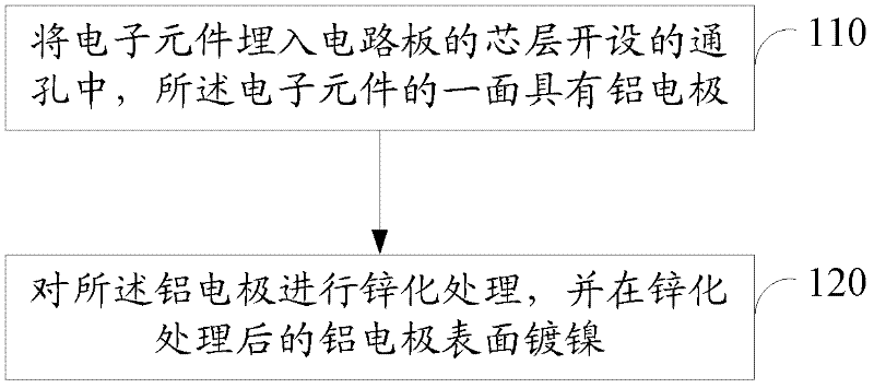
[0017] Please refer to Figure 1a , an embodiment of the present invention provides a method for manufacturing an electronic component embedded circuit board, including:

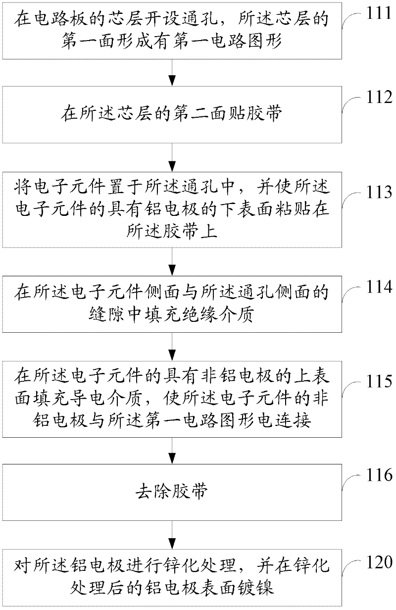
[0018] 110. Embedding electronic components into the through holes opened in the core layer of the circuit board, one side of the electronic components has aluminum electrodes.

[0019] Such ...


PUM


Abstract

The invention discloses a manufacture method of an electronic component embedded type circuit board. The method comprises the following steps: embedding an electronic component into a through hole provided in a core layer of a circuit board, wherein one side of the electronic component is provided with an aluminium electrode; carrying out zinc processing on the aluminium electrode, and plating nickel on a surface of the aluminium electrode after the zinc processing. An embodiment of the invention also provides a corresponding electronic component embedded type circuit board. According to a technical scheme of the invention, the zinc processing and the nickel plating processing are adopted to form a zinc nickel protection layer on the surface of the aluminium electrode. In subsequent circuit board manufacture flows, the aluminium electrode is not damaged by laser, various acidic or alkaline chemical solutions.

Description

technical field [0001] The invention relates to the technical field of circuit board manufacturing, in particular to an electronic component embedded circuit board and a manufacturing method thereof. Background technique [0002] In a conventional power electronic module, a power semiconductor chip, such as a MOSFET or an IGBT chip, is usually connected to a substrate by wire bonding. However, due to its long interconnection size, it is easy to generate large stress and large electromagnetic interference (EMI) noise in the switching power supply. In addition, with the rapid development of power electronic semiconductor devices, the switching frequency is getting higher and higher, the size of the device is further reduced, the influence of parasitic parameters on the performance and reliability of the power supply is becoming more and more significant, and the power consumption of the device is also increasing. . Embedding the power chip directly inside the printed circuit...

Claims


Application Information

Patent Timeline
IPC IPC(8): H05K3/30H05K1/18
CPCH05K2203/1469H01L24/19H01L2924/13055H01L2224/04105H01L2924/13091H05K3/0035H05K2201/10166H05K3/32H05K1/185H05K2201/0347H05K2203/0191H05K1/18H01L21/568H01L23/13H01L23/3121H01L23/5389H01L24/05H01L24/20H01L2224/05124H01L2224/05655H01L2224/92244H01L2924/00H01L2924/0103
Inventor 谷新霍如肖丁鲲鹏杨之诚孔令文蔡坚鲍平华
Owner SHENNAN CIRCUITS
Why Eureka
Try Eureka