Display device and manufacturing method thereof

A technology for a display device and a manufacturing method, applied in nonlinear optics, instruments, optics, etc., can solve problems such as height difference, poor adhesion of light-shielding tape and outer pin bonding area, increased damage to thin film transistor glass substrates, etc.

Inactive Publication Date: 2012-01-04
AU OPTRONICS (XIAMEN) CORP +1
View PDF4 Cites 7 Cited by
  • Summary
  • Abstract
  • Description
  • Claims
  • Application Information

AI Technical Summary

Problems solved by technology

[0004] However, due to the thickness of the lower polarizer attached under the TFT glass substrate, there is a height difference between the Outer Lead Bonding (OLB) region of the TFT glass substrate and the lower polarizer.
Therefore, when the light-shielding tape is attached under the glass substrate of the TFT and the lower polarizer, the height difference between the outer lead bonding area and the lower polarizer will cause poor adhesion of the light-shielding tape and the ou

Method used


Image

  • Display device and manufacturing method thereof
  • Display device and manufacturing method thereof
  • Display device and manufacturing method thereof

Examples


Embodiment Construction

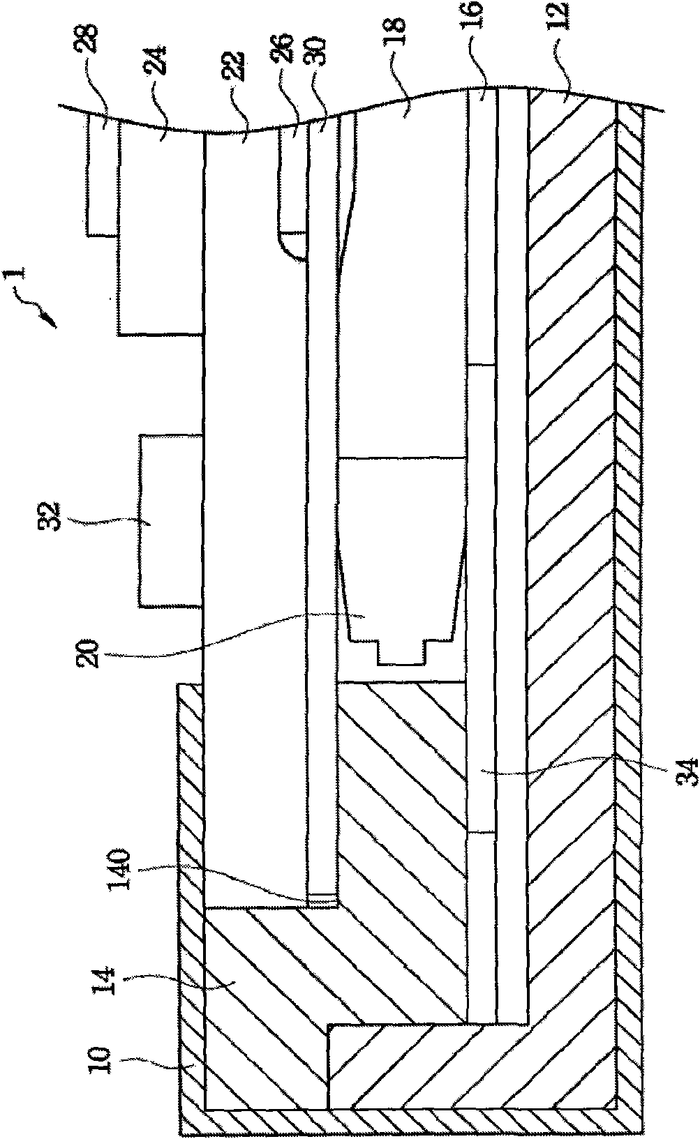
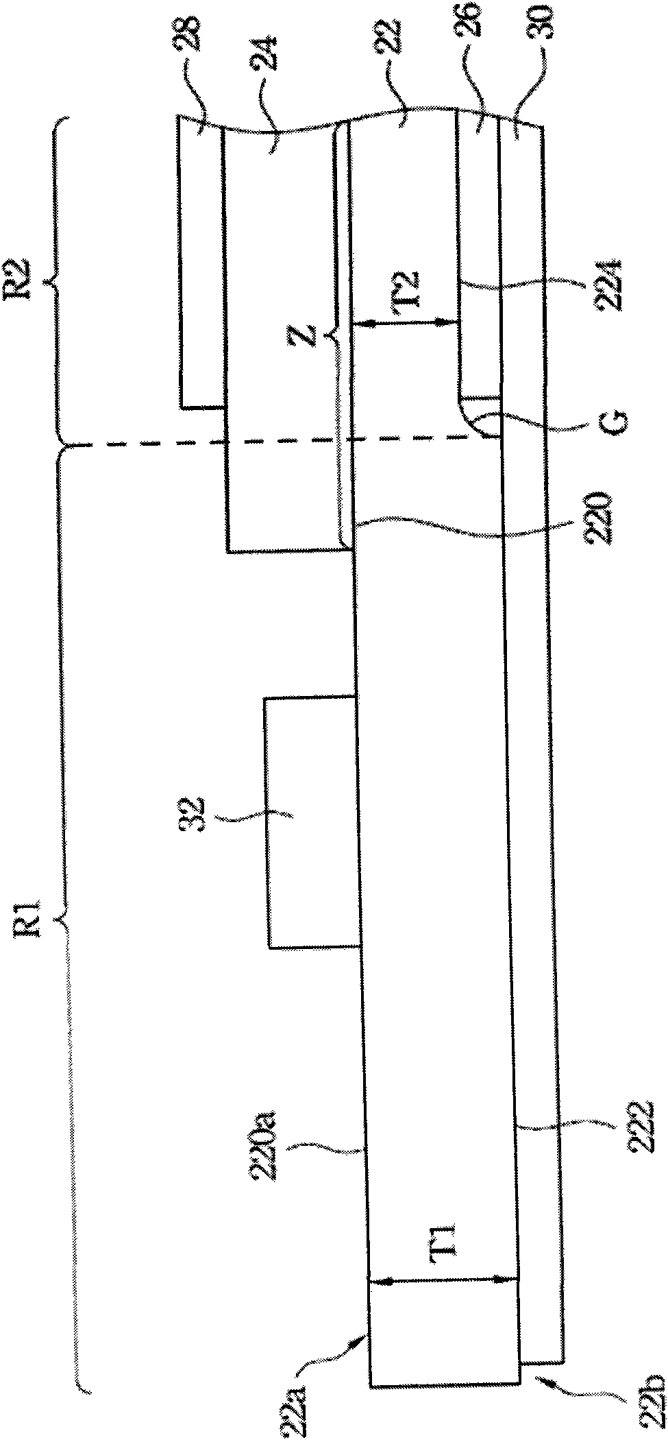
[0028] A plurality of embodiments of the present invention will be disclosed with figures below, and many practical details will be described together in the following description for the sake of clarity. It should be understood, however, that these practical details should not be used to limit the invention. That is, in some embodiments of the present invention, these practical details are unnecessary. In addition, for the sake of simplifying the drawings, some commonly used structures and components will be shown in a simple and schematic manner in the drawings.

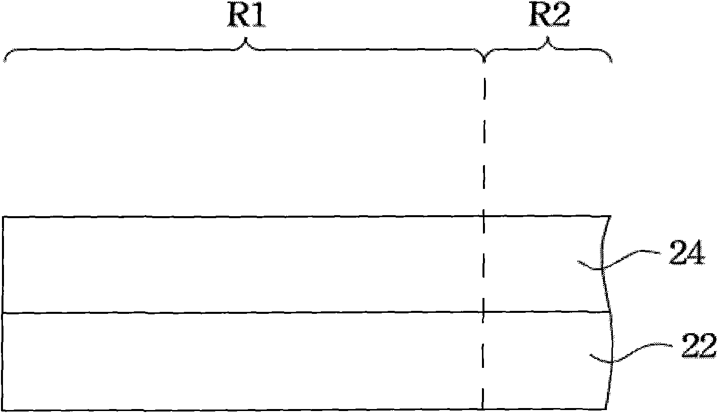
[0029] A technical aspect of the present invention is a display device. More specifically, it is mainly designed to increase the thickness of the color filter glass substrate and the thin film transistor glass substrate in the bonding area of ​​the two without increasing the thickness of the thin film transistor glass substrate in the outer pin bonding area. thickness of. By increasing the thickness of the thin ...


PUM


Abstract

The invention provides a display device, which comprises a first base plate and a second base plate. The first base plate is provided with a first fixed area and a second fixed area. The second base plate is adhered to the first base plate to ensure that a joint surface in the first fixed area is exposed. The second fixed area is positioned in an adhesion area of the first base plate and the second base plate. The first fixed area has a first thickness. The second fixed area has a second thickness. The first thickness is greater than the second thickness to ensure that the first base plate forms a section difference between the first fixed area and the second fixed area. For the display device provided by the invention, the main point is that the thickness of a thin-film transistor glass base plate in an outer pin joint area of the thin-film transistor glass base plate is increased on the basis of not increasing the thicknesses of a colored filter glass base plate and the thin-film transistor glass base plate in the adhesion area of the colored filter glass base plate and the thin-film transistor glass base plate. By increasing the thickness of the thin-film transistor glass base plate in the outer pin joint area of the thin-film transistor glass base plate, a flexible circuit board and an electronic component can be effectively prevented from damaging the thin-film transistor glass base plate when jointed to the outer pin joint area.

Description

technical field [0001] The present invention relates to a display device and a manufacturing method thereof, in particular to a glass substrate of the display device and a manufacturing method thereof. Background technique [0002] In recent years, due to the rapid development of electronics and information industries, the related products have become increasingly sophisticated. As far as the current personal computer field is concerned, in addition to seeking higher-speed, more computing-capable computing units and a variety of peripheral devices to meet the needs of users, the thin and light portable computers are also industry-leading. key areas of development. Taking liquid crystal display as an example, it has the advantages of high image quality, small size, light weight, low voltage drive, low power consumption and wide application range, so it is widely used in portable TVs, mobile phones, video recorders , notebook computers, desktop monitors and other consumer el...

Claims


Application Information

Patent Timeline
IPC IPC(8): G02F1/13G02F1/1333
Inventor 颜华生
Owner AU OPTRONICS (XIAMEN) CORP
Why Eureka
Try Eureka