Field-programmable gate array (FPGA) prototype verification clock device

A clock device and prototype verification technology, applied in the field of FPGA prototype verification, can solve problems such as system resource waste, logic timing tightening, poor stability, etc., and achieve the effect of maximizing the utilization of system clock resources, realizing clock management, and convenient verification

Active Publication Date: 2012-01-04
无锡亚科鸿禹电子有限公司
View PDF2 Cites 16 Cited by
  • Summary
  • Abstract
  • Description
  • Claims
  • Application Information

AI Technical Summary

Problems solved by technology

The irrationality of data transmission and clock strategy leads to low system efficiency and poor stability; in the case of insufficient clock resources, the effective verification logic timing of the FPGA chip is tightened, which cannot meet the needs of customers for high-speed verification. On the other hand, multi-FPGA communication cannot be synchronized, effective, and the bit error rate is high, resulting in a waste of system resources in the verification process

Method used


Image

  • Field-programmable gate array (FPGA) prototype verification clock device
  • Field-programmable gate array (FPGA) prototype verification clock device
  • Field-programmable gate array (FPGA) prototype verification clock device

Examples


Embodiment Construction

[0030] In order to make the above objects, features and advantages of the present application more obvious and understandable, the present application will be further described in detail below in conjunction with the accompanying drawings and specific implementation methods.

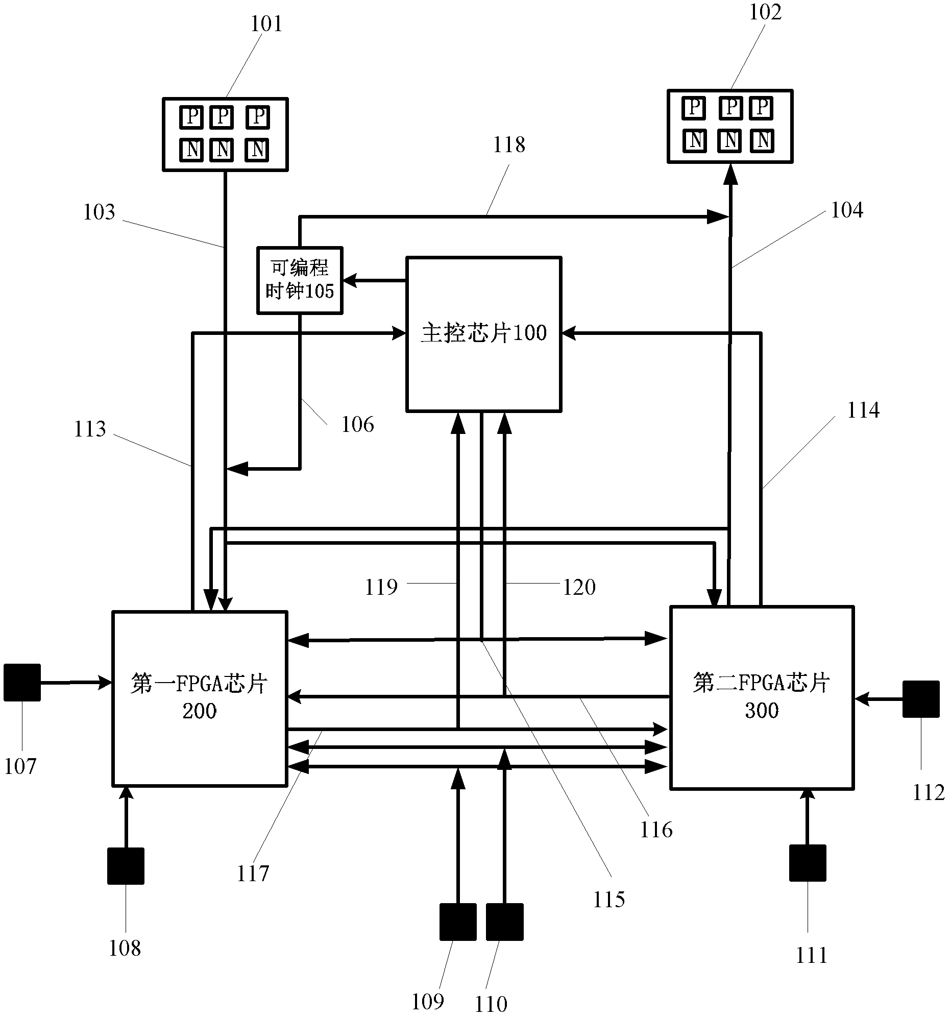
[0031] refer to figure 1 , which shows a schematic structural diagram of a circuit of a preferred FPGA prototype verification clock device of the present application.

[0032] Such as figure 1 , the present application includes a main control chip 100, a first FPGA chip 200, and a second FPGA chip 300;

[0033] And an external clock input and output circuit connected to the first FPGA chip 200 and the second FPGA chip 300 at the same time;

[0034] One end is connected to the main control chip 100, and the other end is respectively connected to the internal programmable clock circuit of the first FPGA chip 200 and the second FPGA chip 300;

[0035] Directly connected to the first FPGA chip 200, or the...


PUM


Abstract

The invention provides a field-programmable gate array (FPGA) prototype verification clock device, and relates to the field of FPGA prototype verification. The device comprises a master control chip, a first FPGA chip, a second FPGA chip, an external clock input / output circuit which is connected with the first FPGA chip and the second FPGA chip simultaneously, an internal programmable clock circuit of which one end is connected with the master control chip and the other end is connected with the first FPGA chip and the second FPGA chip respectively, an external direct-insert crystal oscillator circuit which is directly connected with the first FPGA chip or the second FPGA chip or the first FPGA chip and the second FPGA chip simultaneously, a source synchronous clock circuit which points from the first FPGA chip to the second FPGA chip, and / or a source synchronous clock circuit which points from the second FPGA chip to the first FPGA chip, and a feedback clock circuit which is used for introducing the feedback clock of the first FPGA chip or the second FPGA chip into the master control chip and introducing the adjusted clock into the first FPGA chip and the second FPGA chip. The device realizes the centralized management of various clocks and maximizes a system clock resource utilization rate.

Description

technical field [0001] The present application relates to the field of FPGA prototype verification, in particular to an FPGA prototype verification clock device. Background technique [0002] In the field of FPGA prototype verification, when designing an FPGA prototype verification board, the design of the clock strategy is extremely important. [0003] In the prior art, in the field of FPGA prototype verification, the clock strategies of various verification boards are different, and even the clock pins are wasted; in the clock strategy, a single crystal oscillator is used for the clock, or a single programmable Pll (Phase Locked Loop , phase-locked loop) common method to achieve multiple FPGA clock synchronization; in data transmission, the communication between FPGAs is realized by using the interconnection method of multiple FPGAs. The irrationality of data transmission and clock strategy leads to low system efficiency and poor stability; in the case of insufficient clo...

Claims


Application Information

Patent Timeline
Patent Type & Authority Applications(China)
IPC IPC(8): G06F1/08
Inventor 郭文帅刘永宏
Owner 无锡亚科鸿禹电子有限公司
Why Eureka
Try Eureka