Semiconductor heterostructure diodes

A technology of diodes and transistors, applied in the field of semiconductor electronic devices, can solve problems such as increasing reverse bias current

Active Publication Date: 2012-01-04
TRANSPHORM INC
View PDF6 Cites 25 Cited by
  • Summary
  • Abstract
  • Description
  • Claims
  • Application Information

AI Technical Summary

Problems solved by technology

This drop in the Schottky barrier causes an increased revers...

Method used


Image

  • Semiconductor heterostructure diodes
  • Semiconductor heterostructure diodes
  • Semiconductor heterostructure diodes

Examples


Embodiment Construction

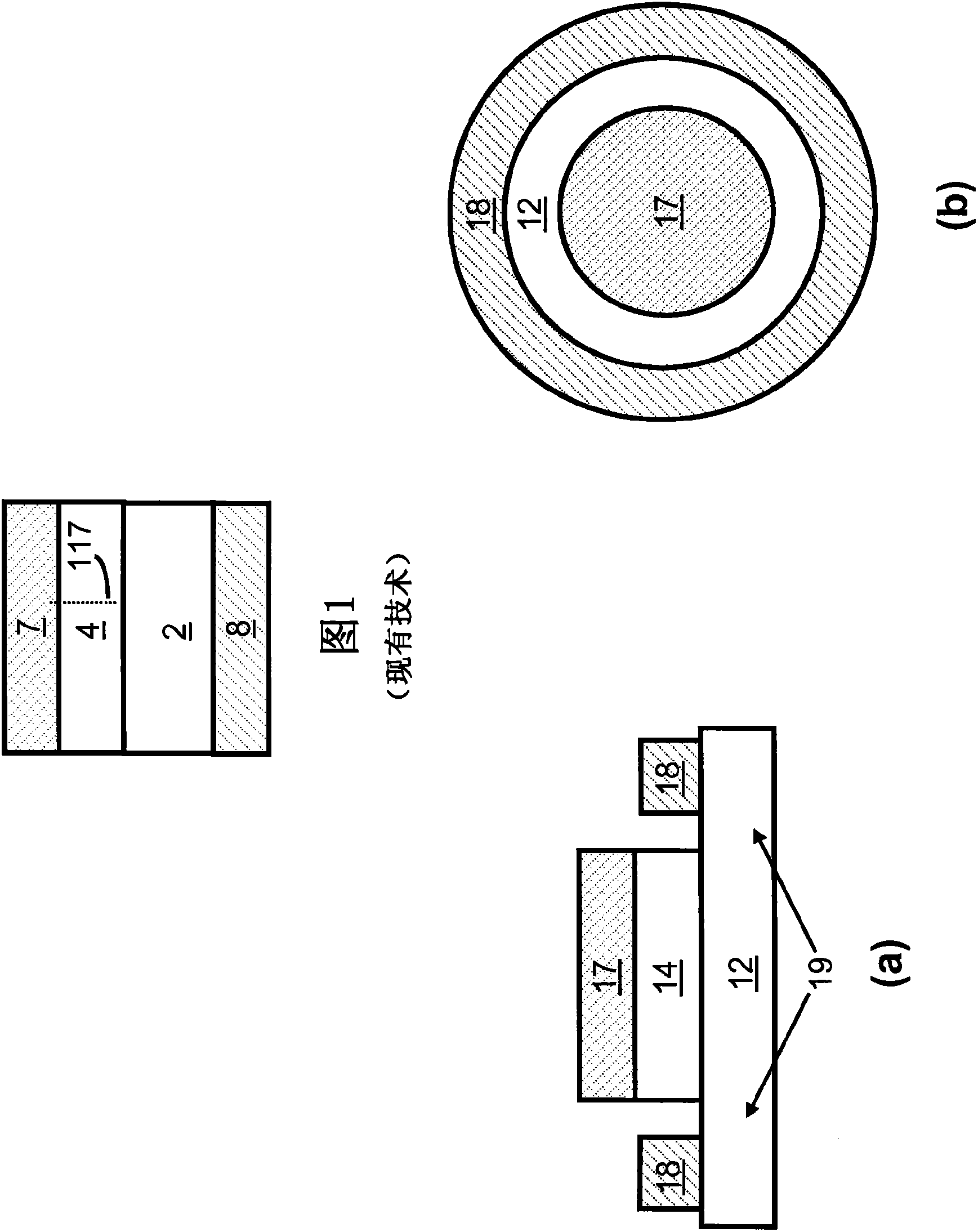
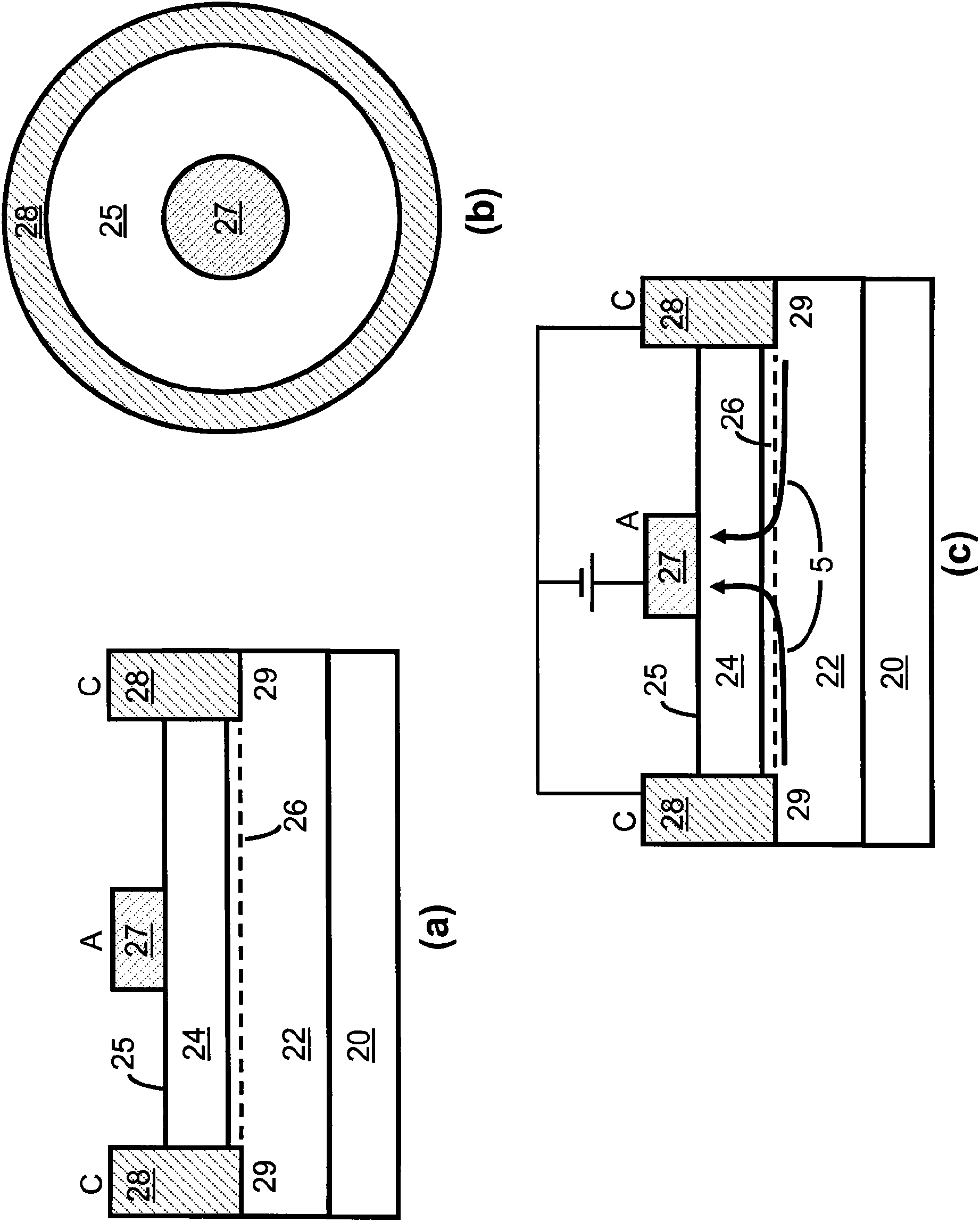
[0045] Described to withstand high reverse voltage while exhibiting low on-resistance R on and diodes based on semiconductor heterostructures with low switching losses. Figure 4 Embodiments of the invention are shown in a and 4b, where Figure 4 a is a cross-sectional view of the present embodiment, Figure 4 b is a plan view (top view) of this embodiment. In short, the semiconductor device of the present embodiment includes a substrate 20, a first semiconductor layer 22 on top of the substrate, and a second semiconductor layer 24 on top of the first semiconductor layer. The semiconductor layers 22 and 24 have compositions different from each other selected such that a two-dimensional electron gas (2DEG) 26 is generated in the first semiconductor layer 22 near the interface between the first and second semiconductor layers 22 and 24 . An anode contact 27 or contacts is formed on top of the surface 25 of the second semiconductor layer 24 and a single cathode contact 28 is form...


PUM


Abstract

Planar Schottky diodes for which the semiconductor material includes a heterojunction which induces a 2DEG in at least one of the semiconductor layers. A metal anode contact is on top of the upper semiconductor layer and forms a Schottky contact with that layer. A metal cathode contact is connected to the 2DEG, forming an ohmic contact with the layer containing the 2DEG.

Description

technical field [0001] The present invention relates to semiconductor electronic devices, in particular to Schottky diodes based on semiconductor heterojunctions. Background technique [0002] Diodes are used in a wide range of electronic circuits. Diodes used in circuits for high voltage switching applications theoretically require the following characteristics. When reverse biased (ie, the cathode is at a higher voltage than the anode), the diode should be able to withstand large voltages while allowing as little current as possible to pass through. The amount of voltage that must be withstood depends on the application; for example, many high power switching applications require the diode to be able to withstand a reverse bias of at least 600V or at least 1200V without significant current flow. When current flows through the diode in the forward direction (from anode to cathode), the forward voltage drop across the diode, V on should be as small as possible to minimize...

Claims


Application Information

Patent Timeline
IPC IPC(8): H01L29/868
CPCH01L29/872H01L29/205H01L29/0615H01L27/0629H01L29/7787H01L29/2003H01L29/4236H01L29/778H01L29/7786
Inventor 吴毅锋乌梅什·米什拉普里米特·帕里克储荣明伊兰·本-雅各布申立坤
Owner TRANSPHORM INC
Why Eureka
Try Eureka