Wide spectrum metal dielectric film grating and optimization method thereof

A technology of metal dielectric and dielectric film, applied in the field of diffraction grating, can solve the problem that it is difficult to obtain diffraction efficiency and anti-laser damage threshold, the bandwidth cannot meet the requirements of femtosecond laser wide spectrum, and cannot meet the requirements of femtosecond laser high diffraction efficiency and other problems, to achieve the effect of high resistance to laser damage threshold, excellent working bandwidth, and reduced difficulty

Inactive Publication Date: 2012-01-11
QINGDAO UNIV
View PDF6 Cites 24 Cited by
  • Summary
  • Abstract
  • Description
  • Claims
  • Application Information

AI Technical Summary

Problems solved by technology

[0004] Although gold-plated grating (Metal grating) has a relatively wide operating bandwidth, it has strong absorption characteristics, and it is difficult to obtain high diffraction efficiency and anti-laser damage threshold
[0005] Multi-layer dielectric grating (Multi-layer dielectric grating, MDG) has the advantages of high diffraction efficiency and high anti-laser damage threshold, but due to the interference of multi-layer dielectric films, its working bandwidth is only limited to tens of nanometers. , and its bandwidth is far from meeting the requirements of femtosecond las

Method used


Image

  • Wide spectrum metal dielectric film grating and optimization method thereof
  • Wide spectrum metal dielectric film grating and optimization method thereof
  • Wide spectrum metal dielectric film grating and optimization method thereof

Examples


Embodiment Construction

[0030] The specific implementation of the present invention will be further described below in conjunction with the accompanying drawings.

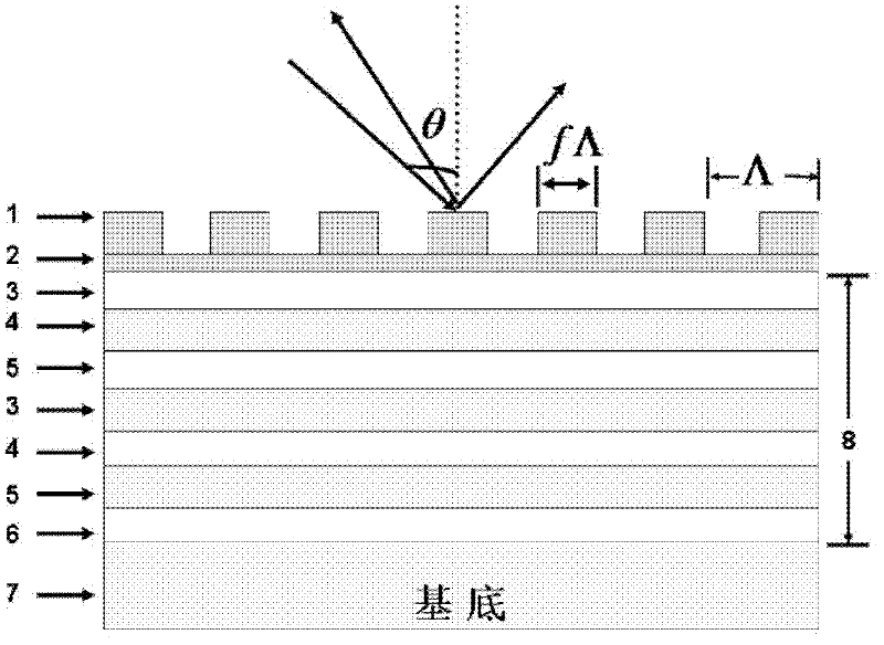
[0031] figure 1 Schematic diagram of the structure principle of the wide-spectrum metal dielectric film grating provided by the present invention, the grating is sequentially composed of a substrate 7, a metal Ag film 6, a SiO 2 Dielectric film 5, HfO 2 Dielectric film 4, TiO 2 Dielectric film 3, remaining film layer 2 and surface grating structure 1; SiO 2 Dielectric film, HfO 2 Dielectric film and TiO 2 The dielectric film forms a multilayer dielectric film in turn, and the metal Ag film and the multilayer dielectric film form a high reflection film 8; the high reflection film 8 formed by the metal Ag film and the multilayer dielectric film can provide high The reflectivity to ensure that the incident light can be fully reflected and diffracted. Above the high reflection film 8 is the remaining film layer 2 after the surface grati...


PUM

PropertyMeasurementUnit
Angle of incidenceaaaaaaaaaa
Thicknessaaaaaaaaaa
Center wavelengthaaaaaaaaaa

Abstract

The invention relates to a wide spectrum metal dielectric film grating and an optimization method thereof; the grating comprises a substrate, a metal Ag film, a multi-layer dielectric film, a residual film layer and a surface grating structure; and every layer of dielectric reflective film comprises a SiO2, a HfO2 and a TiO2 dielectric films. The method first defines a grating diffraction efficiency spectral property value evaluation function, selects the refractive index of metal media and a plurality of layers of dielectric film materials as well as the grating parameters which are optimized, and builds a wide spectrum metal dielectric film grating TE wave diffraction efficiency value analyzing model according to a strict coupled-wave theory. Through the optimization of a plurality of parameters, the obtained grating cycle is 1480lines/mm, the groove depth is 290nm, the thickness of the residual film layer is 10nm, the duty cycle is 0.28, and an incident angle is 60 degrees. According to the invention, when TE polarized light with the wavelength being 1053nm enters, the diffraction efficiency of the wide spectrum metal dielectric film grating in a wide spectrum bandwidth being more than 190nm in the -1 grade direction of reflection diffraction is over 97 percent.

Description

technical field [0001] The invention relates to a wide-spectrum dielectric film grating for a femtosecond chirped pulse amplification system, in particular to a wide-grating high-diffraction-efficiency metal dielectric film grating for a femtosecond laser pulse amplification system with a central wavelength of 1053 nanometers and The optimization method belongs to the technical field of diffraction gratings. Background technique [0002] The performance of the chirped pulse amplification technology (Chirped-pulse amplification, CPA) to obtain ultra-short and ultra-intense laser pulses mainly depends on the pulse width compression grating. The diffraction grating as the core component of the CPA system must have the highest possible diffraction efficiency and The anti-laser damage threshold, which uses a wavelength of 1053 nm and TE mode. [0003] Designing and fabricating pulse width compression gratings with high diffraction efficiency, high damage threshold and wide spect...

Claims


Application Information

Patent Timeline
IPC IPC(8): G02F1/35G02B5/18B32B9/04B32B15/00
Inventor 孔伟金王淑华云茂金王书浩卢朝靖陈沙鸥
Owner QINGDAO UNIV
Why Eureka
Try Eureka