Method for preparing Ge photoelectric detector with transverse p-i-n structure

A p-i-n, photodetector technology, applied in the direction of circuits, electrical components, semiconductor devices, etc., can solve the problem of reducing the light signal responsivity of the device, and achieve the effect of alleviating the requirements of photolithography, small series resistance and improving device performance

Inactive Publication Date: 2014-07-16
XIAMEN UNIV
View PDF4 Cites 16 Cited by
  • Summary
  • Abstract
  • Description
  • Claims
  • Application Information

AI Technical Summary

Problems solved by technology

However, the Ge intrinsic region is also the absorption region of the vertically incident light signal, and the light absorption and the photogenerated carrier transition proceed in the same direction. The thinning of the intrinsic region will inevitably lead to insufficient light absorption at the same time, thus reducing the optical signal response of the device. Spend
The contradiction between high speed and high responsivity is an inherent defect of vertical incidence vertical p-i-n structure Ge photodetectors

Method used


Image

  • Method for preparing Ge photoelectric detector with transverse p-i-n structure
  • Method for preparing Ge photoelectric detector with transverse p-i-n structure
  • Method for preparing Ge photoelectric detector with transverse p-i-n structure

Examples


Embodiment Construction

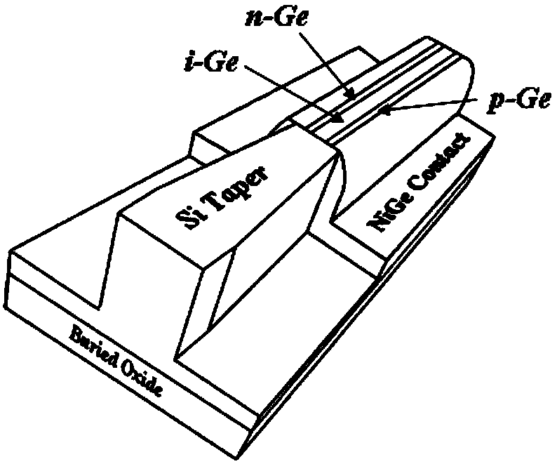
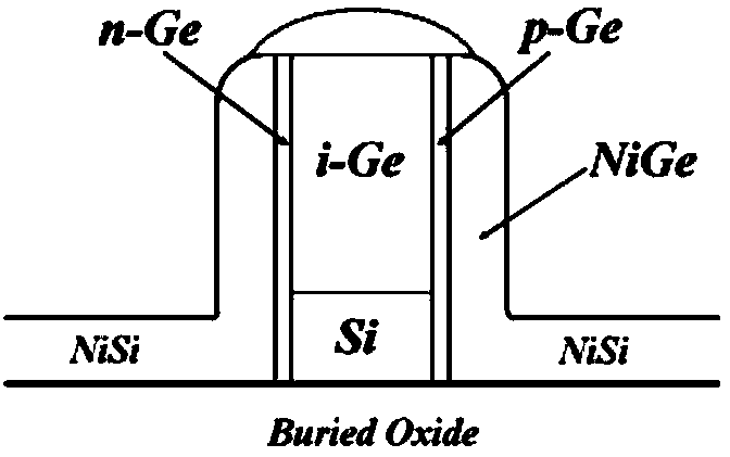
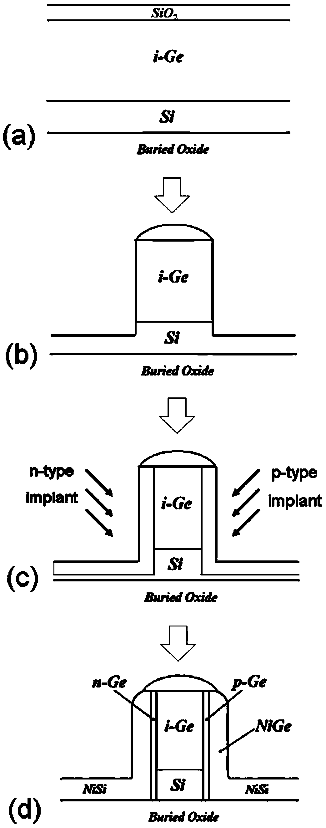
[0023] The invention combines ion direction finding injection and NiGe self-alignment technology, and realizes the preparation of the sub-micron-level line size lateral p-i-n structure Ge photodetector by means of conventional photolithography conditions.

[0024] In step 1), the substrate for Ge epitaxial growth is a silicon-on-insulating SOI substrate. The growth can be obtained by a two-step growth method under ultra-high vacuum conditions, that is, a low-temperature Ge buffer layer of tens of nanometers is formed at a low temperature on a clean Si substrate (low temperature is about 350℃), and then a high temperature is grown on the buffer layer. The Ge layer (high temperature temperature is about 650°C), germane is used as the gas source, and the total thickness of the Ge layer is about 1 μm. The epitaxial germanium layer is then covered with SiO by chemical vapor deposition 2 The thickness of the layer is above 200nm.

[0025] In step 2), use microelectronic lithography tech...


PUM

PropertyMeasurementUnit
Thicknessaaaaaaaaaa
Thicknessaaaaaaaaaa

Abstract

The invention discloses a method for preparing a Ge photoelectric detector with a transverse p-i-n structure, and relates to the germanium photoelectric detector. The method comprises the steps of (1) carrying out epitaxial growth of a monocrystalline germanium layer on a substrate, growing a SiO2 covering layer on the monocrystalline germanium layer, (2) using a micro-electronics photolithography to etch an active area platform surface of a long and thin strip shape on the epitaxial monocrystalline germanium layer, (3) using the SiO2 covering layer on the monocrystalline germanium layer for masking, forming a doped p area and a doped n area on the two sides of the platform surface respectively through sidewise large-declination ion implantation, (4) carrying out thermal annealing after deposition of a metal Ni layer, forming NiGe contact electrodes and NiSi contact electrodes on the two sides of the platform surface and the bottom of the etched area through a self-alignment technology used in the forming process of NiGe and NiSi, and (5) leading out the device electrodes, and protecting a passivating layer. Therefore, the Ge photoelectric detector with the transverse p-i-n structure is obtained. The technology is simple, operability is high, and high application value is achieved.

Description

Technical field [0001] The invention relates to a germanium photodetector, in particular to a method for preparing a Ge photodetector with a lateral p-i-n structure. Background technique [0002] Studies have shown that more than half of the power consumption in integrated circuit chips is concentrated in the interconnection of the chips, and the interconnection is also limited by the signal transmission bandwidth. In the long run, the introduction of optical interconnects in the chip instead of electrical interconnects, and the use of photons as a carrier to achieve high-speed and low-power signal transmission is an inevitable requirement for further integration of the chip. In silicon-based optical interconnection, photodetectors that convert optical signals into electrical signals are important devices for on-chip optical interconnection. The method of making photodetectors is to directly epitaxial germanium (Ge) material on silicon as the active area to prepare long-waveleng...

Claims


Application Information

Patent Timeline
IPC IPC(8): H01L31/105H01L31/18
CPCH01L31/105H01L31/1808Y02P70/50
Inventor 黄巍魏江镔陈松岩李成
Owner XIAMEN UNIV
Why Eureka
Try Eureka